Decoding the AI Full-Stack Approach: Google's Vertical Integration Strategy from Chips to Applications

How Google's vertical integration from custom TPU chips to Gemini models creates a durable AI competitive advantage.
This article dissects Google's AI full-stack strategy—spanning custom TPU hardware, JAX/XLA software frameworks, and Gemini large models. It explains how vertical integration enables cross-layer co-optimization, dramatically reduces inference costs at scale, and accelerates innovation cycles. The piece also examines why only a handful of tech giants can pursue this approach and what it means for the broader AI ecosystem.
What Is the AI Full-Stack Approach?
In the field of artificial intelligence, the term "Full Stack" is frequently mentioned, but what does it actually mean? In simple terms, the AI full-stack approach refers to end-to-end, in-house research and integration of the entire AI technology stack—from underlying hardware infrastructure to upper-layer application software.
This isn't a new concept, but in an era where generative AI is exploding across every domain, it carries more strategic value than ever before. Google has made it clear that the full-stack approach has long been the foundation of its AI efforts—this vertical integration strategy is precisely what underpins its core competitiveness in large-scale model training and efficient deployment.
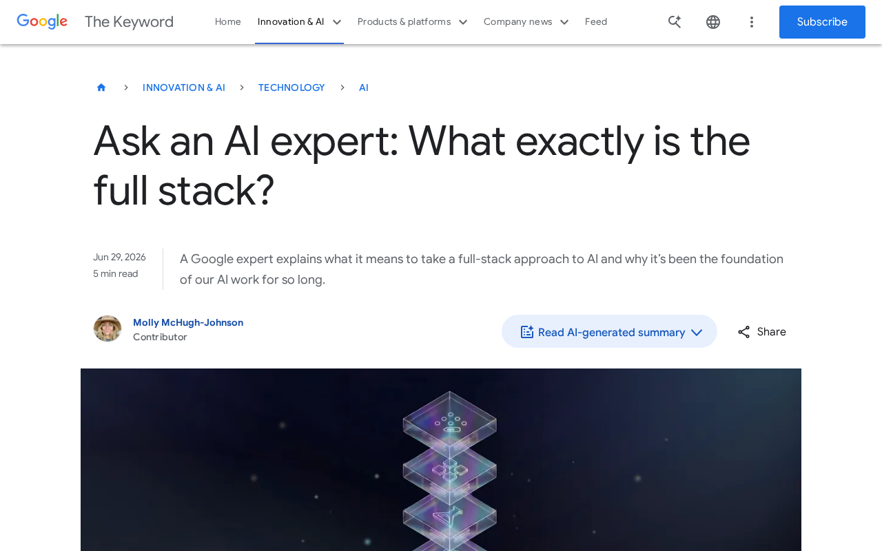
The Layered Structure of the AI Technology Stack
To truly understand the value of full-stack, we first need to clarify what constitutes an AI technology stack. A complete AI technology stack can typically be divided from bottom to top into several key layers.
Bottom Layer: Hardware and Infrastructure
At the very bottom of the technology stack is computing hardware. For AI, this means the design and manufacturing of specialized accelerator chips. Google's in-house TPU (Tensor Processing Unit) is a prime example, purpose-built and optimized for the matrix operations central to deep learning.
Since its first public disclosure in 2016, the TPU has iterated to its fifth generation (TPU v5). Unlike general-purpose GPUs, TPUs employ a Systolic Array architecture specifically designed for hardware-level acceleration of matrix multiplications and convolution operations—the two types of computations that represent the core computational bottlenecks in neural network training and inference. A systolic array consists of thousands of simple multiply-accumulate (MAC) units arranged in a grid, where data flows rhythmically through the array like a heartbeat, eliminating the need to repeatedly access main memory. This dramatically reduces memory bandwidth bottlenecks—which happen to be the primary pain point for GPUs when handling large-scale matrix operations. Data passes between array units in a pipelined fashion, with each unit only needing to perform local multiply-accumulate operations and pass results to its neighbors, thereby achieving ultra-high throughput with minimal memory access overhead. TPUs also integrate High Bandwidth Memory (HBM) and dedicated Inter-Chip Interconnect (ICI) networks, supporting thousands of TPUs forming ultra-large-scale Pod clusters, making it possible to train models with hundreds of billions of parameters. Additionally, this layer encompasses data centers, high-speed network interconnects, cooling systems, and other physical infrastructure. The hardware layer directly determines the upper bound of computing power and unit cost for AI training and inference.
Middle Layer: System Software and Frameworks
Above the hardware sits the system software layer, including compilers, runtime environments, and deep learning frameworks such as TensorFlow and JAX. The core function of this layer is to efficiently map upper-layer model code to underlying hardware for execution.
JAX is a high-performance numerical computing framework developed by Google, regarded as a core component of next-generation deep learning infrastructure. Using NumPy as its interface, it leverages the XLA (Accelerated Linear Algebra) compiler to just-in-time compile (JIT) Python code into efficient hardware instructions, with native support for automatic differentiation, automatic vectorization, and distributed parallelism. Notably, JAX adopts a functional programming paradigm, redefining the deep learning framework development experience through composable transformations (such as grad for gradients, vmap for batch vectorization, and pmap for multi-device parallelism). XLA, as its underlying compiler, performs cross-operation fusion (Op Fusion) on computation graphs, eliminates redundant memory reads and writes, and automatically generates efficient parallel code tailored to specific hardware topologies—enabling the same JAX code to achieve near-theoretical-peak computational efficiency across CPUs, GPUs, and TPUs. The Gemini model family is trained on JAX, which is a direct manifestation of Google's hardware-software co-optimization strategy. By controlling this layer, Google can perform deep customization for its own TPUs, maximizing hardware performance.
Upper Layer: Models and Applications
At the top of the technology stack are the AI models themselves (such as the Gemini family of large models) and the various product applications built on top of these models. This layer directly reaches users and determines how AI capabilities are translated into tangible, perceivable value.
Why Does Google Insist on the Full-Stack Approach?
Cross-Layer Synergy for Ultimate Performance Optimization
The most fundamental advantage of the full-stack approach lies in cross-layer co-optimization. When a single company controls the chips, software frameworks, and model development simultaneously, it can perform joint tuning across layers—guiding chip architecture design based on the computational characteristics of models, and conversely optimizing model structures based on chip capabilities.
This "Hardware-Software Co-design" is a core methodology in chip architecture design, referring to the practice of fully considering upper-layer software and algorithm requirements during the chip design phase, rather than developing them independently and trying to integrate them afterward. Co-design has become a central battleground in AI infrastructure competition: Apple's M-series chips achieve a unified memory architecture across CPU, GPU, and Neural Engine through co-design; Amazon's Trainium and Inferentia chips are custom-designed for dominant cloud workloads; Meta has also developed its in-house MTIA (Meta Training and Inference Accelerator) chip, optimized specifically for its recommendation systems and generative AI models. The common goal of these players is to break through the adaptation limitations of general-purpose computing architectures for specific AI workloads, embedding algorithmic requirements directly into silicon hardware to achieve orders-of-magnitude improvements in energy efficiency. In the era of large models, the deep coupling between model architectures (such as Transformer attention mechanisms) and chip memory bandwidth and computational parallelism makes the benefits of co-design increasingly significant—the performance gains from this integration are simply unattainable by approaches that rely solely on third-party components.
Cost Control at Scale
The training and inference costs of large models are extraordinarily high. Through full-stack in-house development, Google can free itself from dependence on external suppliers and systematically reduce marginal costs.
The unit cost of large model inference is a core variable in AI commercialization, and its importance has become increasingly prominent as large models transition from training to large-scale inference deployment. Training is a one-time or periodic cost, but inference costs grow linearly or even super-linearly with user volume. Taking ChatGPT as an example, its early per-conversation cost was estimated to be dozens of times higher than traditional search. Custom silicon systematically compresses energy consumption and latency per inference by streamlining general-purpose compute units, enhancing hardware acceleration for specific operators, and combining software techniques like quantization and sparsity. Amazon AWS's Inferentia claims up to 70% inference cost reduction compared to equivalent GPU instances. When AI services need to be delivered at scale to billions of users, even a few percentage points of reduction in per-inference cost yields enormous cumulative economic value—for platforms handling billions of daily requests, this difference directly determines the commercial viability boundary of AI services. This is also the fundamental driving force behind why Google, Meta, Microsoft, and other tech giants are all betting on Custom Silicon strategies.
Technical Autonomy and Rapid Iteration
Controlling the complete technology stack also means stronger technical autonomy and faster innovation cycles. When a bottleneck emerges at any layer, a full-stack team can quickly locate and collaboratively resolve it without depending on external suppliers' update cycles. This end-to-end control enables Google to more agilely translate cutting-edge AI research breakthroughs into deployed products.
The Real-World Barriers to the Full-Stack Approach
Of course, a full-stack strategy doesn't come without costs. Independently developing a complete technology stack requires sustained massive capital investment and world-class talent—chip design, compiler engineering, distributed systems, large model research—each field is its own deep domain with extremely scarce and highly specialized talent. This is a barrier that the vast majority of companies cannot overcome. In fact, even financially strong mid-sized tech companies can often only make limited in-house investments in one or two layers of the technology stack. This explains why only a handful of tech giants like Google, Amazon, and Microsoft possess the capability to execute a truly full-stack strategy.
For most enterprises and developers, the more pragmatic path is to stand on the shoulders of these full-stack platforms, building their own AI applications through cloud services and open APIs. A deep understanding of the full-stack approach's logic helps us make more informed decisions when choosing technology partners, and more clearly identify the real technical differences behind various AI services.
Conclusion
The full-stack approach represents a philosophy of vertical integration from chips to applications. As the AI race continues to intensify, whoever can better control the complete technology stack will establish lasting advantages in performance, cost, and innovation speed. Google's positioning of full-stack as the cornerstone of its AI strategy reflects its recognition of the long-term competitive moat built through end-to-end integration. For practitioners following the direction of the AI industry, understanding the full-stack concept is an essential lens for gaining insight into how the industry landscape is evolving.
Key Takeaways
Related articles
Harness Engineering: The Core Infrastructure for Taking AI Agents from Demo to Production
Deep dive into Harness Engineering: why AI Agents need memory management, durable execution, guardrails & approvals to go from demo to production.

Claude Code vs Codex: Hands-On Comparison and Installation Guide for AI Programming Tools
In-depth comparison of Claude Code and Codex AI programming tools covering accuracy, installation, and network setup tips to help developers choose the best solution.

GPT-5.6 Free Trial Is a Scam: How to Spot AI Marketing Traps
Exposing the "GPT-5.6 free trial" scam circulating on social media. Learn about data risks of third-party AI mirror platforms and how to identify AI marketing traps.