Did AI Really Design a Chip? Breaking Down the Truth Behind OpenTPU

OpenTPU is an open-source AI accelerator on an off-the-shelf FPGA — not a chip AI autonomously designed.
The viral claim that "AI autonomously created a chip" stems from the OpenTPU project, but the reality is far more modest: it's an open-source AI accelerator design running on an existing Kintex 7 FPGA — a very different thing from fabricating a new chip. The project's real value is its fully open toolchain covering hardware code, instruction set, simulator, compiler, and profiler. Its key engineering insight is that token generation is bottlenecked by memory bandwidth, not compute — a fundamental constraint in modern AI hardware. The "AI involvement" and performance claims also lack independent verification, and the project is nowhere near a substitute for NVIDIA GPUs.
Where Did the "AI Made a Chip" Claim Come From?
A viral video posed an attention-grabbing question: did AI actually design its own chip? The short answer — it's not that simple. The project at the center of the discussion is OpenTPU, an open-source AI accelerator design. The project's author claimed AI was involved in its development, and that was enough to send the "AI made a chip" narrative spreading rapidly.
But look at the technical details, and the reality is far more measured. The demo doesn't run on a newly manufactured chip — it runs on an off-the-shelf Kintex 7 FPGA board. FPGAs are programmable hardware that can be reconfigured through code, but that is a completely different thing from "taping out and fabricating a brand-new chip."
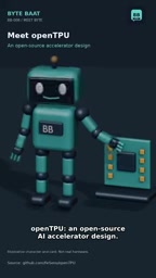
In other words, this is AI-assisted design of an accelerator that runs on programmable hardware — not AI conjuring a chip fabrication plant out of thin air. Conflating the two is the biggest misreading in how this story spread.
What OpenTPU Actually Opens Up
OpenTPU's real value lies in its openness. The project doesn't just drop a black box — it publishes the core components of the entire stack: hardware code, the instruction set, a simulator, a compiler, and a profiler.

This means researchers and developers can get a complete picture of an AI accelerator, from hardware description all the way up to the software toolchain. For anyone learning hardware design or exploring accelerator architectures, this kind of end-to-end open-source material is more educationally and academically valuable than a "chip" alone.
The combination of an FPGA and an open-source toolchain lowers the barrier to experimentation — you don't need millions of dollars in tape-out costs to validate an accelerator design idea on programmable hardware. That has always been the core appeal of the open-source hardware ecosystem.
The Technical Lesson Worth Remembering
Set aside the marketing hype, and this project delivers one genuinely useful engineering insight. The author reports that token generation speed is bottlenecked by memory bandwidth, not raw compute.

This is a recurring bottleneck in modern AI hardware design: moving data is often more expensive than doing the math. Many people assume running large models is primarily a floating-point compute problem, but in practice the overhead of shuffling weights and intermediate results on and off the chip frequently becomes the decisive constraint. This is exactly why High Bandwidth Memory (HBM) is so critical in AI accelerators.
Understanding this point is useful whenever you encounter hype about "next-generation AI chips" — peak compute figures alone tell you very little. The memory subsystem design matters just as much.
HBM (High Bandwidth Memory) stacks multiple layers of DRAM dies vertically using Through-Silicon Vias (TSVs) and places them in close proximity to the processor via 2.5D packaging. Compared to conventional GDDR memory, HBM uses an extremely wide physical bus — 1024 bits or wider — delivering far greater memory bandwidth at relatively low clock frequencies. During large language model inference, every generated token requires loading the model's full weights from memory; the larger the model and the narrower the memory bandwidth, the more pronounced the throughput bottleneck becomes. This is the fundamental reason why high-end AI accelerators like NVIDIA's H100 integrate HBM3 regardless of cost. For resource-constrained open-source projects or edge devices, memory bandwidth hits its ceiling far sooner than compute — a real-world engineering truth that OpenTPU's benchmarks confirm.
These Claims Still Need Independent Verification
Two caveats must be stated clearly. First, the claim that "AI participated in development" is currently only the author's own account; it has not been independently reviewed, and just how much AI actually contributed to the design remains unclear. Second, performance and speed claims equally need independent testing to back them up.
More importantly, this project is in no way evidence of a "replacement for NVIDIA." It is an open-source accelerator design with educational and research value, running on programmable hardware — not a new chip poised to disrupt the industry.
Conclusion: Tell the Real Story Accurately
OpenTPU is an open-source project worth paying attention to. It publishes a complete toolchain and surfaces memory bandwidth as a critical bottleneck. But it is neither a chip autonomously created by AI nor a challenge to the existing GPU giants.
When reporting on tech news, accuracy matters more than sensationalism. The honest narrative is this: AI assisted in designing an accelerator that runs AI, deployed on an off-the-shelf FPGA — and nothing more. Respecting those boundaries is what gives people a clear-eyed understanding of where AI and hardware development actually stand.
Background: An FPGA (Field-Programmable Gate Array) is a chip whose logic circuits can be reconfigured repeatedly after it leaves the factory. Unlike ASICs (Application-Specific Integrated Circuits), an FPGA's interior consists of a large array of programmable logic cells and configurable interconnects. Engineers write code in a hardware description language such as Verilog or VHDL, then go through synthesis, place-and-route, and other steps to "program" the design onto the device. The Kintex 7 is a mid-to-high-end FPGA series from Xilinx (now acquired by AMD), commonly used in prototyping, communications, and image processing. Because FPGAs can run any digital circuit design without tape-out, they are an ideal platform for chip architecture research and teaching — designers can iterate and validate ideas quickly without bearing the millions of dollars in cost and months of lead time that tape-out demands.
Related articles

Should U.S. College Fraternities Be Banned? A Researcher's Incisive Observations
Why not just ban U.S. college fraternities? A researcher finds the key resistance comes from decision-makers' own fraternity identities and schools' "willful ignorance."

Microsoft Discovery: Accelerating Scientific Discovery with AI Agents
Microsoft's Discovery platform runs specialized AI agents to help researchers screen and prioritize the most promising compounds and experimental paths, reducing experiments and accelerating scientific discovery.

Cambridge Heavy Industries Secretly Develops Desktop-Scale Nuclear Fusion Device
Cambridge Heavy Industries is secretly developing a desktop-scale laser-driven nuclear fusion device, targeting the equipment supply market for fusion power plants. This article analyzes its miniaturization technology path, commercialization logic, and unique positioning in the fusion startup wave.