SK Hynix's Record $26.5B IPO: The AI Memory Chip Boom and the U.S. Factory Chess Game

SK Hynix's record $26.5B IPO spotlights the AI memory boom and U.S. pressure on Korean chipmakers to build local fabs.
Korean memory giant SK Hynix raised $26.5 billion in the largest-ever U.S. IPO by a foreign company, fueled by surging HBM demand for AI. The article explores HBM's technical moat, the memory industry's cyclical risks, the U.S. CHIPS Act guardrails pressuring Korean firms to build local fabs, and the broader geopolitical restructuring of the semiconductor supply chain.
The AI Chip Boom Spawns Wall Street's Largest-Ever Foreign IPO
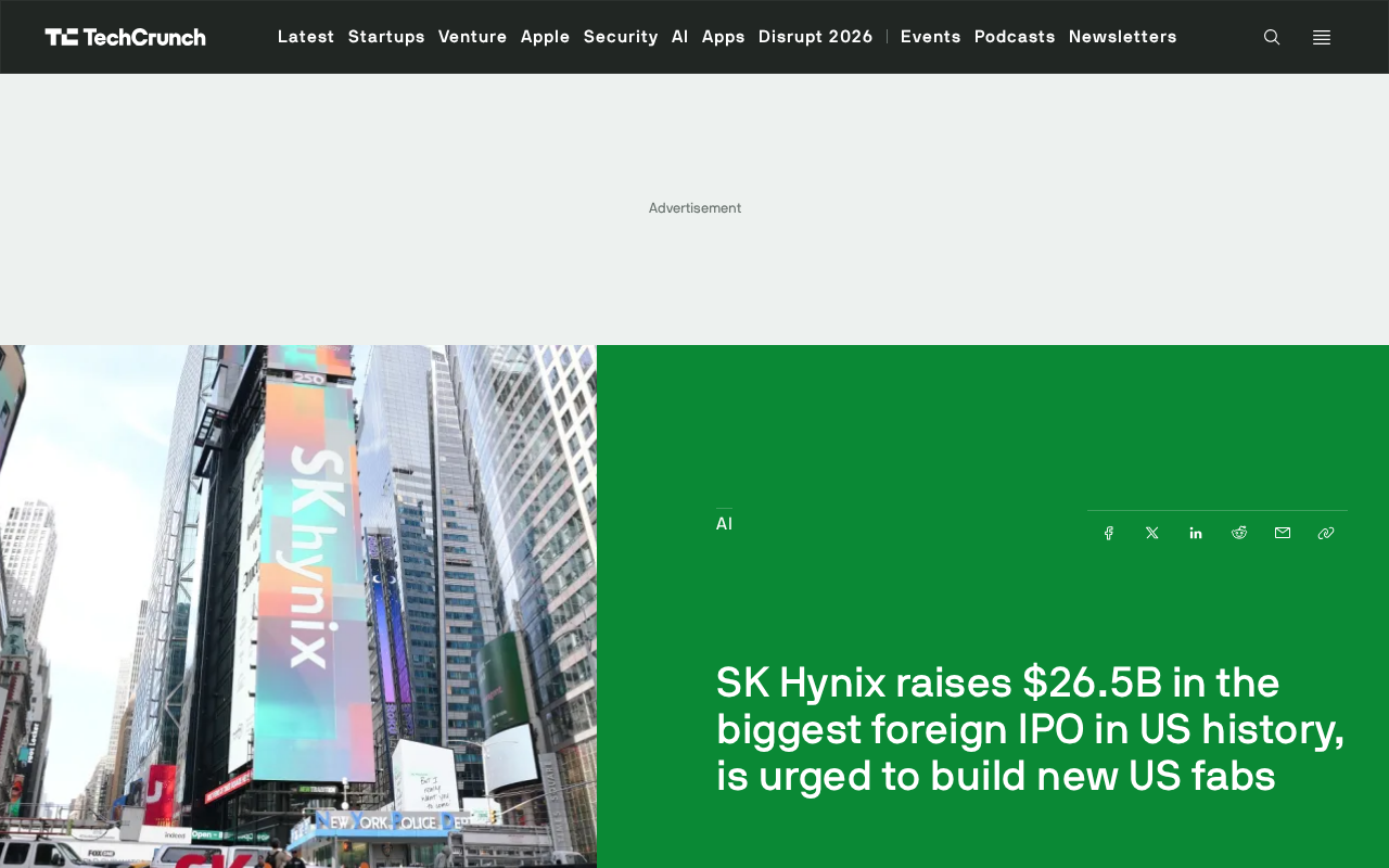
The AI chip boom is reshaping the global semiconductor landscape in unprecedented ways, and the latest footnote to this trend has emerged on Wall Street. According to foreign media reports, Korean memory chip giant SK Hynix successfully raised $26.5 billion, setting a record for the largest IPO by a foreign company in U.S. history. This milestone not only reflects capital markets' high optimism about AI memory demand, but also marks the global semiconductor supply chain's formal entry into a new cycle driven by AI compute.
For SK Hynix, this massive fundraising comes at just the right time. As a leading supplier in the global high-bandwidth memory (HBM) market, SK Hynix is an irreplaceable key link in NVIDIA's AI accelerator supply chain. As the demand for memory bandwidth from large model training and inference climbs sharply, HBM has leapt from a relatively niche product to a core component that determines the performance ceiling of AI chips. Capital markets' embrace of this narrative is directly reflected in the record-setting fundraising scale.
Notably, SK Hynix's choice to list in the United States rather than conduct a secondary offering in its home market of Korea is itself a decision with profound strategic implications. U.S. capital markets place a significantly higher valuation premium on AI infrastructure concepts than Asian markets, and institutional investors on Nasdaq and the NYSE possess a historically high depth of understanding and willingness to allocate to the semiconductor industry. Furthermore, a U.S. listing helps SK Hynix forge tighter capital-level ties with core customers like NVIDIA, Microsoft, and Google, strengthening its strategic positioning as a "member of the U.S. AI ecosystem"—an identity that carries strategic value beyond the commercial level in the current geopolitical context.
Why Memory Chips Have Landed at the Center of the AI Wave
Over the past two years, market attention has largely focused on GPUs and AI accelerators, with NVIDIA at one point becoming the world's most valuable company. But the industry has gradually realized that the bottleneck of AI compute lies not solely in the computing units themselves—the Memory Wall problem is equally fatal.
The so-called memory wall refers to the long-standing gap between processor computing speed and memory access speed. This concept was first formally introduced by William Wulf and Sally McKee in their 1995 paper "Hitting the Memory Wall: Implications of the Obvious." Its fundamental cause is that improvements in CPU/GPU computing speed follow Moore's Law, doubling performance every 18-24 months, while DRAM latency improves at only about 7% per year, and bandwidth growth also lags far behind compute growth. In the era of large models, this contradiction has been sharply amplified: the attention mechanism of the Transformer architecture must repeatedly read the KV Cache (key-value cache) during the inference phase, and its memory access pattern is characterized by high randomness and low reuse rates, consuming far more memory bandwidth than traditional deep learning workloads. Research shows that in large language model inference, more than 70% of the time may be spent waiting on memory access rather than on actual computation.
As GPU compute grows rapidly following Moore's Law, DRAM bandwidth improvements lag far behind, causing computing units to spend large amounts of time in a data-"starved" state waiting for data. In large model inference scenarios, since model parameter scales reach tens of billions or even hundreds of billions, memory access becomes a severe bottleneck—take GPT-3 as an example: its 175 billion parameters require about 350GB of memory at float16 precision, far exceeding the memory capacity of a single GPU. This makes high-bandwidth, large-capacity HBM a core constraint in AI chip design, and is the fundamental driving force behind why mainstream AI accelerators like NVIDIA, AMD, and Google TPU have all adopted HBM solutions.
High Bandwidth Memory (HBM) vertically stacks multiple layers of DRAM chips and achieves high-density inter-layer interconnection through Through-Silicon Via (TSV) technology, providing bandwidth far exceeding that of traditional memory. The implementation of TSV technology is extremely precise: it requires etching deep holes only a few microns in diameter into the silicon wafer (with an aspect ratio typically exceeding 10:1), then filling them with conductive copper to form vertical interconnect channels. A hole-diameter deviation exceeding 0.1 microns can lead to poor contact, and in a 12-layer DRAM stack, the failure of a TSV in any single layer can render the entire HBM module scrap. Multi-layer chip stacking also faces stress concentration issues caused by CTE (Coefficient of Thermal Expansion) mismatch, which must be mitigated through precise thermal management design and underfill materials. Compared to traditional GDDR6 memory, HBM offers 3-5 times higher memory bandwidth while consuming less power and occupying a smaller package footprint. HBM is typically installed side-by-side with a GPU or AI accelerator on the same silicon interposer through 2.5D packaging technology, greatly shortening the data transmission path—the HBM interface bus width of NVIDIA's H100 reaches 5,120 bits, far exceeding the 384 bits of traditional memory. HBM has now iterated to the HBM3E generation, and SK Hynix was the world's first manufacturer to mass-produce HBM3E, with its products widely adopted in NVIDIA's H100/H200 series GPUs, making it one of the biggest beneficiaries of this wave.
Looking ahead to the next generation, HBM4 is expected to enter mass production in 2025-2026. Its core breakthrough lies in the base die adopting a more advanced process (expected around 4nm level) and introducing a design that doubles the I/O interface width (expanding from 1,024 bits to 2,048 bits), with theoretical peak bandwidth potentially exceeding 1.5TB/s. Even more disruptive technical directions are Near-Memory Computing and Processing-in-Memory (PIM): the former integrates some computing logic directly onto the HBM base die, while the latter embeds computing circuits alongside the DRAM memory cell arrays, fundamentally eliminating the overhead of moving data between memory and computing units. Samsung has released an HBM-PIM prototype with PIM functionality, and SK Hynix's AiM (Accelerator-in-Memory) architecture is also exploring a similar path. If in-memory computing achieves large-scale commercialization, it will have a profound impact on the existing separated GPU-HBM architecture, redefining the performance bottlenecks and supply chain landscape of AI chips.
HBM's high technical barriers are particularly evident in yield economics, which is also the core of its moat. Take HBM3E 12-Hi (12-layer stack) as an example: a single module contains tens of thousands of TSV interconnect points, and a failure at any single point renders the entire module scrap. The industry estimates that for every 1 percentage point increase in HBM yield, the corresponding cost per GB can drop by about 2-3%. The yield advantage SK Hynix has accumulated in mass-producing HBM3E is the core confidence behind its ability to lock in long-term supply agreements with NVIDIA at more competitive prices. Samsung's HBM4 is expected to enter mass production in 2025, at which point the yield competition among the three players will further intensify, and yield management capability will become a key variable determining shifts in market share.
It is worth noting that the physical integration of HBM and GPU relies on advanced packaging platforms such as TSMC's CoWoS (Chip-on-Wafer-on-Substrate). CoWoS integrates GPU chips and HBM memory side-by-side through a silicon interposer, shortening the inter-chip connection distance from centimeters to microns, making ultra-wide buses possible. Technical routes competing with CoWoS also include Intel's Foveros 3D packaging, Samsung's X-Cube, and TSMC's own SoIC 3D packaging solution. In 2023-2024, CoWoS capacity was severely short, at one point becoming the actual bottleneck for NVIDIA H100 shipments—even when chip production itself was sufficient, deliveries could not be made on time due to insufficient packaging capacity. This phenomenon has prompted many countries to incorporate advanced packaging into the core support scope of their semiconductor subsidy policies.
SK Hynix's competitive landscape in the HBM market is also worth attention. Globally, SK Hynix, Samsung, and Micron are the only three suppliers capable of mass-producing HBM. According to data from market research firm TrendForce, SK Hynix has long maintained a market share above 50%; Samsung's share is around 40%, but it once lagged behind in yield and product maturity; Micron is a rising star, with its HBM3E products already certified for NVIDIA's H200. The production barriers for HBM are extremely high: TSV process precision requirements are extremely demanding, and the more stacked layers (currently mainstream at 12 layers), the exponentially harder yield control becomes, requiring deep coordination with advanced packaging capabilities, giving the HBM market a naturally highly oligopolistic competitive structure.
This $26.5 billion fundraising will inject ample ammunition into SK Hynix's capacity expansion plans and next-generation HBM R&D, further consolidating its leading position in the high-end memory chip market.
U.S. Ramps Up Pressure: Urging Korean Firms to Build Domestic Factories
However, capital market success is only half the story. Reports indicate that alongside SK Hynix completing this landmark fundraising, the United States is actively urging SK Hynix and another Korean memory giant, Samsung, to build new fabs on U.S. soil.
Behind this demand is the semiconductor industry localization strategy the United States has continuously pushed in recent years. The CHIPS and Science Act, signed into effect in August 2022, adopts a multi-layered architecture of parallel incentives and constraints in its policy design. At the direct subsidy level, the CHIPS Program Office under the U.S. Department of Commerce is responsible for allocating $39 billion in manufacturing subsidies; applicant companies must submit detailed business plans, labor agreements, and supply chain information, with an approval cycle lasting 12-18 months. At the tax incentive level, the act provides a 25% Investment Tax Credit (ITC) for newly built or expanded semiconductor manufacturing facilities, one of the largest tax breaks for a single industry in U.S. history. The act also includes "guardrail provisions": companies receiving subsidies may not build or expand advanced chip capacity in China or other "countries of concern" for 10 years—subsidized companies that expand mature-process (above 28nm) capacity by more than 10% in countries of concern, or engage in any advanced-process (below 28nm) capacity expansion, must return all subsidies.
From publicly disclosed negotiation cases, the actual enforcement of the guardrail provisions has considerable flexibility, but the pressure is real. TSMC's two fabs in Arizona (N4P and N3 processes) have secured approximately $6.6 billion in subsidy commitments from the U.S. Department of Commerce, but during negotiations TSMC engaged in arduous talks over a capacity exemption for its Nanjing plant in China, ultimately securing a limited-term capacity maintenance exemption. Samsung's fab in Taylor, Texas has secured approximately $6.4 billion in subsidies, but its Xi'an NAND plant in China similarly faces long-term constraint pressure from the guardrail provisions. SK Hynix has announced plans to build an advanced packaging plant in Indiana and applied for related subsidies, but the treatment of its Wuxi DRAM plant remains a core sensitive point in negotiations. These cases show that the guardrail provisions are not a one-size-fits-all ban, but rather a dynamic lever the U.S. government uses to continuously influence the global investment decisions of subsidized companies—its pressure effect continues to ferment both during the subsidy application review period and during the compliance oversight period after subsidy agreements are signed.
This provision essentially places the global investment decisions of subsidized companies under U.S. government supervision, creating real pressure for companies like Samsung and SK Hynix—Samsung's NAND Flash plant operating in Xi'an, China accounts for about 40% of its total global NAND capacity, and SK Hynix's DRAM plant in Wuxi is also pivotal. How to strike a balance between accepting U.S. subsidies and maintaining existing capacity in China is a core issue in the repeated back-and-forth of the two companies' negotiations over building U.S. factories. Companies including TSMC, Samsung, Intel, and Micron have all announced plans to build U.S. factories, with cumulative investment exceeding $400 billion. The backdrop to this act was the fragility of the global chip supply chain exposed during the COVID-19 pandemic, as well as the U.S.'s high vigilance toward the geopolitical risk surrounding Taiwan; its essence is to position the chip industry as a strategic resource directly tied to national security. At a time when AI is viewed as the core of national strategic competition, memory chips, as a key component of AI infrastructure, naturally become a focus of policy attention.
Viewed from the perspective of the Korean government, this chess game of building factories in the U.S. also touches domestic policy nerves. Korea has long supported the capital expenditures of its two memory giants through R&D tax credits, low-interest industrial policy loans, and preferential land supply, viewing their dominance as a core pillar of national economic security. SK Hynix's decision to list in the U.S. and accept the constraints of the U.S. policy framework has sparked domestic debate in Korea about whether core technology assets are being excessively tilted toward U.S. interests. Combined with the implicit constraints the U.S. "guardrail provisions" impose on Korean firms' China operations, Seoul must strike a precise diplomatic and policy balance among alliance relations, industrial interests, and corporate operational autonomy—the complexity of this multi-party game far exceeds the scope of pure commercial decision-making.
The Multiple Games Behind the Factory Decision
For SK Hynix and Samsung, building factories in the U.S. is a complex strategic puzzle. On the plus side, the U.S. market is enormous, geographically close to core customers like NVIDIA and AMD as well as hyperscale cloud providers, and local capacity helps shorten supply chain response cycles and meet customers' urgent demand for supply security.
But the challenges are equally undeniable: the cost of building factories in the U.S. is significantly higher than in Korea and other parts of Asia, and the maturity of talent reserves and supporting industry chains remains a real threshold. More critically, memory chips are a capital-intensive and highly cyclical industry. Memory chips (DRAM and NAND Flash) are one of the most cyclically volatile segments of the semiconductor industry, dubbed the "hog cycle" by the industry, and its formation mechanism has deep economic roots: demand is highly fragmented (consumer electronics, servers, phones, etc.), while supply is highly concentrated among a few oligopolies. More critically, there is an inherent 18-24 month lag between capacity expansion decisions and capacity coming online, a lag determined jointly by fab construction cycles (usually over 18 months) and equipment delivery cycles (the backlog period for key equipment such as lithography machines sometimes exceeds 12 months). When market prices rise, all major manufacturers launch expansion almost simultaneously, and 18 months later the concentrated release of new capacity often causes severe oversupply; a price crash triggers industry-wide production cuts, which also have a lag, causing prices to continuously overshoot before bottoming out. This "cobweb effect" is especially extreme in the memory industry—in 2022-2023 alone, the average NAND Flash price fell more than 60%, the average DRAM price at one point dropped 75%, and SK Hynix, Samsung, and Micron all recorded quarterly losses in the billions of dollars. It was only from 2024, driven by AI demand, that the industry returned to a boom cycle.
Aggressive capacity expansion during periods of surging AI demand seems to go with the flow, but once market supply and demand reverse, the massive U.S. capacity investment could turn into a heavy financial burden—this is a hidden concern that Korean manufacturers must weigh carefully before making commitments.
The Geopolitical Restructuring of the AI Supply Chain
This event reflects a more macro structural trend: AI is no longer merely a technological and commercial issue, but is deeply embedded in geopolitical maneuvering. From GPU export controls to advanced-process restrictions, to today's strong demand for domestic memory chip capacity, the global semiconductor supply chain is undergoing a round of deep restructuring oriented toward national security and technological sovereignty.
It is worth mentioning that advanced packaging capability is becoming a new strategic battleground in this restructuring. Advanced packaging technology is being upgraded from a "supporting process" of semiconductor manufacturing to a core link that determines a chip's performance ceiling. TSMC's CoWoS packaging platform is currently the most mainstream 2.5D packaging solution, and its capacity has long been in short supply, becoming yet another bottleneck constraining AI chip shipments. In the field of true 3D die-stacking packaging (vertically stacking logic chips and memory chips), the competition is even more intense, with the potential to boost memory bandwidth by another order of magnitude. The U.S. CHIPS Act has specifically allocated $3 billion for advanced packaging R&D, and Japan is also heavily investing in packaging capability through the Rapidus project. The essence of this competition is that countries have realized: even if they master the most advanced chip designs, without corresponding packaging capability, the final product's performance will still be severely constrained—packaging has become a technological sovereignty element as important as lithography, and countries including the U.S. and Japan have incorporated advanced packaging capability into the key scope of their semiconductor industry support policies, meaning that future competition dimensions will extend from pure chip manufacturing to the entire packaging ecosystem.
Korean companies occupy a delicate position in this restructuring: they are both indispensable suppliers to the U.S. AI ecosystem and need to maintain a commercial balance between the U.S. and China. SK Hynix's choice to list in the U.S. and raise a huge sum of money can also be seen as a strategic signal of its proactive move to deepen ties with U.S. capital markets and the industrial ecosystem.
Far-Reaching Implications for the Global Semiconductor Industry
For observers of the AI industry, this series of developments conveys several clear signals:
- The compute arms race is going full-chain: competition over AI compute is extending across the entire chain—memory, advanced packaging, interconnect, and more—and a single-point technical breakthrough is no longer enough to define the competitive landscape;
- Geographic distribution of capacity becomes a strategic variable: fab location strategy is now on par with technical strength, becoming an equally important competitive chip;
- An unprecedented fundraising window: capital markets' high valuations of AI infrastructure provide relevant companies with a rare strategic financing opportunity.
In the coming years, whether SK Hynix and Samsung will build U.S. fabs at scale, and at what pace, will become a key barometer for observing the direction of the global AI supply chain. This concerns not only the fate of the two Korean giants, but will also profoundly affect the cost structure and supply stability of the entire AI hardware ecosystem.
Conclusion
SK Hynix's record-setting $26.5 billion IPO is the latest and most powerful footnote the AI chip boom has cast in capital markets. And behind the U.S.'s urging to build domestic factories lies the increasingly complex geopolitical and industrial game deep within this boom. As memory chips move from behind the scenes to center stage, HBM technical barriers, packaging capacity bottlenecks, and cyclical risks together form the underlying variables of this race. The balance of power in the global semiconductor industry is also quietly being recalibrated. Every participant caught up in it will seek its own foothold amid the parallel tracks of opportunity and risk.
Related articles

AI Writes Code, Will Programmers Lose Their Jobs? The Truth About Devin's Autonomous Programming
Devin and other autonomous AI coding agents are changing software development: from Copilot-assisted coding to fully automated engineering agents, the programmer's role shifts from writing code to system design and oversight. This article analyzes the impact of AI programming on employment, code security, and junior developer training, as well as the real direction of programmer demand under the efficiency paradox.

Citigroup's 14,000 Engineers Use Devin, Slashing Tech Outsourcing Bill by 30%
Citigroup's 14,000 engineers used AI coding agent Devin to cut its tech vendor bill by 30% and speed releases 30-40%, while JPMorgan says AI gains aren't in earnings yet.

AGENTS.md in Practice: Making Coding Agents Actually Work
AGENTS.md and CLAUDE.md can boost coding agent performance, but research shows misuse raises costs 20%. Here's what to write, what to delete, the 200-line and 32KB limits, monorepo nesting rules, and a security warning.