30 Million USD in Funding: The Ambition and Challenge of Redesigning the CPU
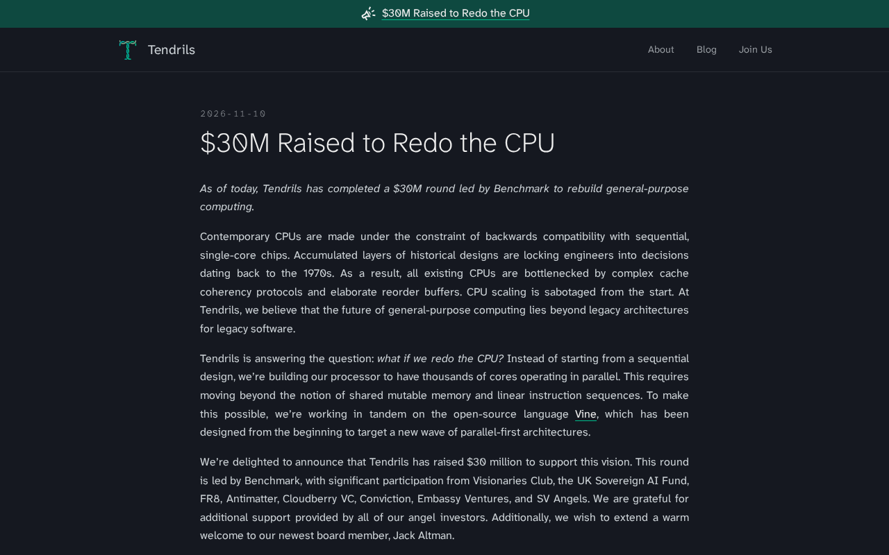
A startup has raised 30 million USD to redo the CPU, prompting reflection on computing architecture innovation.
A startup has announced 30 million USD in funding aimed directly at redesigning the CPU, drawing attention on Hacker News but not intense discussion. The article analyzes possible instruction set-level rethinking and the route battle between specialization and generalization. In chip design, 30 million USD is early-stage capital and is more likely to be used for architecture validation and prototyping rather than direct mass production. The original information did not disclose the technical route, team background, or product timeline, and the market remains in a wait-and-see state. If significant advantages can be proven in specific scenarios, it may open a new path between general-purpose CPUs and specialized accelerators, making it worth the continued attention of developers and technical decision-makers.
Why Would Anyone Want to Redesign the CPU?
In the chip industry, CPU architecture evolution has followed two main lines—x86 and ARM—for decades. Although performance keeps improving, the underlying design paradigm has not fundamentally changed. Now, a startup has announced 30 million USD in funding with the goal of "redesigning the CPU." This news has drawn attention on Hacker News. Although discussion is not yet heated, the direction itself is worth examining in depth.
According to information on Hacker News, the 30 million USD in funding will support CPU redesign. Although the original text did not disclose the specific technical roadmap, team background, or product timeline, the proposition of "redoing the CPU" itself touches on several core tensions in computing architecture: the balance between generality and specialization, the historical baggage of instruction sets, and the trade-off between energy efficiency and performance.
What Does Redoing the CPU Mean?
Rethinking at the Instruction Set Level
Traditional CPU design is constrained by backward compatibility. The x86 architecture carries decades of instruction set legacy, and although ARM has achieved great success in mobile, its design philosophy is likewise rooted in general-purpose computing. Redesigning the CPU may mean making different choices at the instruction set level—for example, a more aggressive reduced instruction set, extensions for specific workloads, or an entirely new parallel execution model.
A funding scale of 30 million USD is not large in the chip design field. For an advanced-process CPU, going from design to tape-out to mass production often requires hundreds of millions of dollars in investment. Therefore, this funding is more likely to be used for early architecture validation, prototype development, or customized design for niche scenarios, rather than directly challenging general-purpose CPU giants.
Instruction Set Architecture (ISA) is the contract between software and hardware, defining the set of instructions a CPU can understand, the register model, and memory addressing modes. x86 is a complex instruction set (CISC), while ARM and RISC-V are reduced instruction sets (RISC). Once an ISA is established, it creates massive software ecosystem lock-in: operating systems, compilers, and applications are all compiled for a specific ISA. If redesigning the CPU changes the ISA, it means the entire software stack must be rebuilt, which is an extremely high ecosystem barrier. Therefore, most CPU startups choose to remain compatible with existing ISAs (for example, RISC-V is open but still requires ecosystem development) or define new ISAs in specific domains.
The Route Battle Between Specialization and Generalization
In recent years, the rise of specialized accelerators (such as GPUs, TPUs, and NPUs) has challenged the position of general-purpose CPUs. One possible direction for redesigning the CPU is to stop pursuing the ability to "do everything" and instead deeply optimize for specific workloads (such as AI inference, data processing, and edge computing). This approach is similar to the rise of the RISC-V ecosystem—lowering the barrier to innovation through an open instruction set and making customization possible.
However, the original information on Hacker News did not indicate whether this company is using RISC-V or another open architecture. Lacking these details, we can only infer its possible technical path from industry trends.
RISC-V is an open-source, open instruction set architecture initiated by the University of California, Berkeley in 2010. Unlike x86 and ARM, which require licensing, anyone can freely use RISC-V to design chips, greatly lowering the barrier to innovation. RISC-V allows developers to add custom instruction extensions, making it particularly suitable for specialized designs. In recent years, the RISC-V ecosystem has developed rapidly, expanding from embedded systems to data centers and AI acceleration. However, RISC-V is still in its early stages in general-purpose high-performance computing, and its software ecosystem and toolchain are not yet mature. This is one of the main challenges facing startups adopting this architecture.
Funding and Team: The Key Variables for Success or Failure
For a chip startup, 30 million USD is seed capital, not a decisive chip. Historically, many CPU startups have fallen due to broken funding chains or tape-out failures. Successful cases often have two characteristics: first, the team has deep microarchitecture design experience; second, it has found early customers or partners willing to share risk.
Because the original material did not provide team background information, it is impossible to judge its technical strength. But what is certain is that in the current chip startup ecosystem, investors are becoming more cautious about grand narratives such as "redoing the CPU." The 30 million USD funding amount shows that capital is willing to bet, but it also sets clear milestone expectations.
Tape-out refers to the process of submitting a designed chip layout to a wafer foundry for manufacturing. For advanced processes (such as 5nm and 3nm), tape-out costs are extremely high: a single set of masks alone may cost millions to tens of millions of dollars, and with wafer manufacturing and packaging and testing, the total cost of a single tape-out can reach tens of millions of dollars. If design defects are found after tape-out, another tape-out is required, doubling the cost. Therefore, 30 million USD in funding is indeed limited for advanced-process CPU design and is more likely to be used for FPGA prototype validation, simulation, or small-scale trial production on mature processes, rather than directly targeting the most advanced processes.
Industry Impact and Observations
If this company can prove in specific scenarios that a redesigned CPU has significant advantages (for example, a substantial improvement in energy efficiency or an order-of-magnitude lead in processing speed for specific workloads), it may open a new path between general-purpose CPUs and specialized accelerators. Conversely, if it merely repeats existing design ideas, it will be difficult to establish a foothold in a chip market dominated by giants.
For developers and technical decision-makers, this event is worth keeping an eye on. The innovation cycle for CPU architecture is long, but once a viable alternative emerges, the optimization logic of the entire software stack may change with it.
Conclusion
Redesigning the CPU with 30 million USD in funding is a bold starting point. The original information is limited, but it is enough to prompt thinking about the future of computing architecture. In the tug-of-war between specialization and generalization, this company's success will depend on its choice of technical route, team execution, and ecosystem-building capability. The low level of discussion on Hacker News may indicate that the market is still watching, but every architecture-level attempt in the chip industry deserves serious attention.
One-line Summary
A startup has raised 30 million USD to redo the CPU, prompting reflection on innovation in computing architecture.
Paragraph Summary
A startup has announced 30 million USD in funding aimed directly at redesigning the CPU. The news drew attention on Hacker News, but discussion has not been intense. The article analyzes the possible rethinking at the instruction set level involved in redoing the CPU, as well as the route battle between specialization and generalization. In chip design, 30 million USD is early-stage capital and is more likely to be used for architecture validation and prototype development rather than direct mass production. The original information did not disclose the technical route, team background, or product timeline, and the market remains in a wait-and-see state. If the company can demonstrate significant advantages in specific scenarios, it may open a new path between general-purpose CPUs and specialized accelerators, which is worth the continued attention of developers and technical decision-makers.
Related articles

Fable 5.2's Self-Improvement Loop Accelerates as Gemini 4 Carbon Closes In
Anthropic Fable 5.2 and Google Gemini 4 Carbon launch together, Remote Labor Index doubles, self-improvement loop accelerates, but benchmark flaws and evaluation awareness persist.

Meta FAIR Releases e-means: A New k-means Alternative That Converges 10x Faster
Meta FAIR releases e-means in FAISS 1.16.0, replacing mini-batch k-means with ~10x fewer epochs, 10-45x GPU speedup, and no new hyperparameters.

AI Is Great at Writing Code, So Why Are Codebases Becoming More Fragile?
AI coding tools boost efficiency but may make codebases fragile. Based on a developer blog and Hacker News discussion, this article analyzes the hidden costs of AI-generated code, community divisions, and practical suggestions for reducing risks.