Does PCIe 4.0 x8/x8 Slow Down Dual-GPU Local LLM Inference?

PCIe 4.0 x8/x8 has limited impact on dual-GPU 70B local inference, with only 3%–6% throughput loss.
The article uses a counterintuitive conclusion to debunk the myth that dual-GPU workstations must use x16/x16. In tensor parallel (TP=2) mode with vLLM or llama.cpp, the real bottleneck in autoregressive decoding is GPU memory bandwidth (936–1008 GB/s), not PCIe bus bandwidth. Tensor parallelism only transmits intermediate activation tensors across the bus, just 32–64 KB per layer per token. The real challenge is synchronization latency from AllReduce operations; at batch size = 1, latency dominates, so x8 and x16 perform similarly.
Bottom Line First: x8/x8 Doesn't Seriously Slow Down Local Inference
Many dual-GPU workstation builders are willing to spend thousands of extra dollars just to run two GPUs on a pure x16/x16 server motherboard, assuming that halving the PCIe lanes means halving token throughput. This assumption ignores how Transformers actually work.
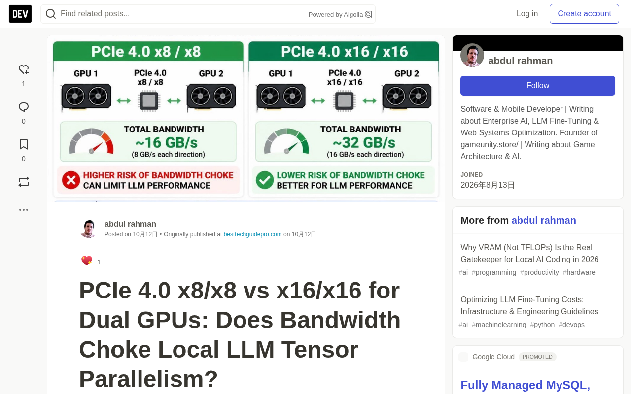
In Tensor Parallel (TP=2) mode with engines like vLLM or llama.cpp, PCIe 4.0 x8/x8 does not significantly bottleneck single-stream token generation. PCIe 4.0 x16 offers about 31.5 GB/s unidirectional bandwidth, x8 about 15.75 GB/s; but the real bottleneck in autoregressive decoding is GPU memory bandwidth (936–1008 GB/s), not the bus. In real-world tests, a 70B model running across dual GPUs on x8/x8 versus x16/x16 typically shows a throughput loss of only 3%–6%. Only under high-concurrency batch serving or the prefill stage of extremely long prompts does the x8 split introduce measurable NCCL AllReduce latency overhead.
What Tensor Parallelism Actually Transmits
A common misconception is that running a local LLM means the GPU is constantly shuttling tens of GB of model weights over PCIe. That's not the case.
In tensor parallel mode, model weights are already sharded and resident in each GPU's memory before inference begins. What actually crosses the bus are the intermediate activation tensors during the forward pass, not the weights.
Take a 70B model with hidden dimension 8192 and batch size = 1: roughly only 32 to 64 KB of activation data is transferred per layer per token generated. Across 80 layers, the total data crossing PCIe per token is only a few MB. Sending 5 MB over a 15.75 GB/s link takes less than 0.3 milliseconds—far below human perception and nearly indistinguishable from x16.
Tensor Parallelism (TP) is fundamentally about splitting the weight matrices within a single Transformer layer along a dimension, assigning each GPU a portion to compute, and then stitching the partial results back together via collective communication. In the classic scheme proposed by Megatron-LM, the Q/K/V projections in multi-head attention are split by attention head, while the two linear layers of the MLP alternate between column and row splitting, so each card holds roughly half the weights, nearly halving memory usage. The cost is that each layer's forward pass must insert synchronization operations like AllReduce or AllGather to align results across the two cards before proceeding to the next layer. Thus, tensor parallelism's communication frequency scales with model depth, and it is far more sensitive to cross-GPU communication latency than pipeline parallelism. This is the key to understanding the whole article: TP's bottleneck has never been the data volume per transfer, but the number of synchronizations multiplied by the inherent latency of each.
The Real Bottleneck Is Sync Latency, Not Bandwidth
Activation data is small, but the real challenge in multi-GPU inference is synchronization. Tensor parallelism requires two AllReduce operations per layer.
According to NVIDIA NCCL documentation, collective communication on consumer-grade multi-GPU topologies involves: kernel launch overhead on both GPUs, packet traversal latency through the PCIe root complex (about 1.5–2.5 microseconds), and CUDA synchronization barriers.
In small-message exchange scenarios with batch size = 1, the dominant factor is latency, not bandwidth, so x16 doesn't significantly reduce latency versus x8. Both experience the same root complex switching latency.
AllReduce is a collective communication primitive that sums tensors element-wise across all participating GPUs and broadcasts the result back to each card. In tensor parallelism, it appears at the concatenation points of attention and MLP, so the more layers, the denser the calls. AllReduce performance is characterized by two quantities: algorithm bandwidth (algbw), reflecting effective throughput for large messages; and bus bandwidth (busbw), multiplied by a topology factor for cross-hardware comparison. When messages are below a certain threshold (typically tens to hundreds of KB), communication enters the latency-dominated regime, where bandwidth is nearly irrelevant and performance is determined by kernel launch, PCIe link handshake, and synchronization barriers. NCCL uses Ring or Tree algorithms on PCIe-only topologies, often choosing Tree for small messages to reduce hop count. Understanding the latency-dominated regime explains why x8 and x16 perform similarly at batch size = 1.
Pipeline Parallelism vs Tensor Parallelism: When Bus Speed Matters
When scaling local LLMs across multiple GPUs, there are two architectural choices with completely different sensitivity to PCIe.
Pipeline Parallelism (PP): Layers 1–40 on GPU 0, layers 41–80 on GPU 1, each token crosses PCIe only once at the boundary layer. It is almost completely immune to lane bandwidth—x8/x8 or even x4 works; the cost is idle bubbles as the two cards wait for each other.
Tensor Parallelism (TP): Both cards compute every layer simultaneously, no idle bubbles, single-token latency halved, but each token requires 160 AllReduce synchronizations. If batch size scales beyond 16 for enterprise serving, the x8 link will eventually saturate.
The Motherboard Lane Tax: From B650 to TRX50
Consumer desktop CPUs provide only 16–24 dedicated PCIe lanes, and dual-GPU configurations fall into roughly three categories.
Consumer split (x8/x8): Motherboards like the ASUS ProArt X670E-Creator or MSI MEG Z790 ACE split the CPU's 16 lanes into two x8 slots, with both cards directly connected to the CPU for lowest latency. Total motherboard cost is about $450–600.
Budget trap (x16 CPU / x4 chipset): Cheaper B650 or Z790 boards route the first card through the CPU (x16) and the second through the chipset (x4). This configuration should be avoided entirely—chipset routing introduces severe DMI bus latency, and tensor parallel speed drops by over 35%.
High-end workstation (true x16/x16): AMD Threadripper 7000 (TRX50) or Intel Xeon W provide 48–112 dedicated lanes, enabling full-speed x16/x16 for dual cards. Complete platform cost is about $2500–4500.
Going with Threadripper specifically for dual x16/x16 is a very capital-inefficient investment. That $2500 premium would be better spent on a higher-tier GPU, faster memory, or cloud compute.
The distinction between CPU-direct lanes and chipset lanes is the most easily overlooked pitfall when choosing a board. Modern consumer CPUs (like AM5's Ryzen 7000/9000, LGA1700's Core) provide only 20–28 PCIe lanes, of which 16 are dedicated to graphics slots. When a motherboard claims dual-GPU support, there are usually two paths: either split the CPU's 16 lanes into x8/x8 with both cards directly connected to the CPU; or let the first card take x16 exclusively while the second hangs off the chipset (like AMD Promontory, Intel PCH), connecting back to the CPU via DMI or a similar link. Chipset downstream bandwidth is typically only PCIe 4.0 x4 level, and shared with other peripherals. This is why x16/x4 chipset routing collapses under tensor parallelism—it lacks bandwidth and adds extra DMI forwarding latency. When buying a dual-GPU motherboard, always confirm the second slot's lane source is the CPU, not the chipset.
NVLink Bridge: Why Dual 3090s Beat Dual 4090s
Discussing dual-GPU interconnect bandwidth inevitably brings up the NVLink Bridge.
The RTX 3090 is the last consumer card with a physical NVLink interface. Two 3090s with a bridge achieve 112.5 GB/s bidirectional bandwidth—over seven times that of PCIe 4.0 x8 and nearly four times x16.
NVIDIA deliberately removed NVLink from the RTX 4090 to protect profit margins on its data center products. As a result, two 4090s can only use PCIe. Although the 4090 has stronger FP8 compute, in tensor parallel inference, dual 3090s with an NVLink bridge have lower collective communication overhead.
NVLink is NVIDIA's point-to-point high-bandwidth interconnect bus, independent of PCIe, allowing GPUs to directly read and write each other's memory, with hardware-level atomic operations and memory consistency. On Ampere consumer cards, NVLink 3.0 provides about 14.0625 GB/s unidirectional bandwidth per link (about 28 GB/s bidirectional total), and the RTX 3090 supports dual-link bridging, yielding about 56 GB/s unidirectional, 112.5 GB/s bidirectional aggregate. Besides higher bandwidth, NVLink's other advantage is lower latency and no PCIe root complex traversal, which benefits small-message AllReduce significantly. NVIDIA completely removed NVLink from Ada-architecture RTX 40 series, officially citing insufficient consumer demand, but the industry widely believes it relates to product tiering strategy for data center A100/H100. Thus, used dual 3090s with an NVLink bridge remain a highly cost-effective combination for small-scale multi-GPU inference.
Interconnect Architecture Comparison Matrix
| Bus Topology | Unidirectional Bandwidth | Typical Platform | 70B TP=2 Relative Speed | Engineering Conclusion |
|---|---|---|---|---|
| PCIe 4.0 x8 / x8 | 15.75 GB/s | AM5 / Z790 split | 3.9% slower than x16/x16 | Best value for single-machine coders |
| PCIe 4.0 x16 / x16 | 31.5 GB/s | Threadripper / Xeon W | Baseline (100%) | Excellent, but high motherboard tax |
| PCIe 4.0 x16 / x4 (chipset) | ~3.9 GB/s | Cheap B650 / low-end Z790 | 34.5% slower | Must avoid for tensor parallelism |
| Dual 3090 + NVLink bridge | 56.25 GB/s | Any dual-GPU board | 6.2% faster than x16 | DIY golden solution |
| PCIe 5.0 x8 / x8 | 31.5 GB/s | Next-gen motherboards | Equivalent to PCIe 4.0 x16 | Future-proof standard |
Frequently Asked Technical Questions
Does PCIe 4.0 x8/x8 bottleneck dual-GPU local LLM inference? Single-stream token generation (batch size = 1) is not significantly limited. The throughput gap between x8/x8 and x16/x16 is typically within 3%–5%, because generation is mainly constrained by GPU memory bandwidth (936–1008 GB/s), not PCIe.
How much bandwidth difference is there between x8 and x16? PCIe 4.0 x16 has about 31.5 GB/s theoretical unidirectional bandwidth (63 GB/s bidirectional); split into x8, the unidirectional link ceiling is exactly halved to about 15.75 GB/s.
Is NVLink required for dual-GPU tensor parallelism? No. Modern engines like vLLM support tensor parallelism over standard PCIe P2P DMA. But dual 3090s with an NVLink bridge provide 112.5 GB/s bidirectional bandwidth, nearly eliminating cross-GPU synchronization latency.
Is it worth buying an expensive workstation motherboard for x16/x16? For 70B local inference, no. Upgrading from an x8/x8 consumer motherboard to an expensive Threadripper platform costs thousands of dollars for less than 5% improvement in token generation speed.
The complete testing methodology, NCCL telemetry, and topology data are published on CERN Zenodo (DOI: 10.5281/zenodo.22641931), with all conclusions from actual hardware tests in vLLM and llama.cpp environments.
One-line Summary
PCIe 4.0 x8/x8 has limited impact on dual-GPU 70B local inference, with only 3%–6% throughput loss.
Paragraph Summary
The article uses a counterintuitive conclusion to debunk the myth that dual-GPU workstations must use x16/x16. The author points out that in tensor parallel (TP=2) mode with vLLM or llama.cpp, the real bottleneck in autoregressive decoding is GPU memory bandwidth (936–1008 GB/s), not PCIe bus bandwidth. Tensor parallelism only transmits intermediate activation tensors across the bus, just 32–64 KB per layer per token, totaling only a few MB across 80 layers; an x8 link at 15.75 GB/s completes this in under 0.3 milliseconds. The real challenge is the synchronization latency from two AllReduce operations per layer. At batch size = 1, latency dominates, and x8 vs x16 makes little difference. Only when batch scales beyond 16 for enterprise serving will x8 saturate. The article also compares pipeline parallelism, the chipset x4 trap, NVLink, and various motherboard platforms, ultimately recommending spending budget on stronger GPUs or cloud compute rather than expensive workstation motherboards.
Related articles

FastAPI: A High-Performance Python Framework and a Production-Ready API Development Powerhouse
FastAPI is a high-performance web framework based on Python type hints, supporting async and automatic OpenAPI docs. With over 100k GitHub stars, this article analyzes its core strengths, production readiness, and selection advice.

Tesla Optimus Begins Mass Production: Can the Goal of 20,000 Units Per Week Be Achieved?
Tesla Optimus officially begins mass production as Musk sets a target of 20,000 units per week. This article analyzes the supply chain challenges behind mass production, the real gap in capacity ramp-up, and the competitive landscape for humanoid robots.

PCL: A Minecraft Launcher with 8.5k Stars — Why Was It Written in VB.NET?
An in-depth analysis of PCL, the GitHub Minecraft launcher with 8,500+ stars: why it chose VB.NET, its features and China network advantages, and the limits of Windows-only.