Microsoft's Maia 300 Custom AI Chip Unveiled: Targeting Multi-Gigawatt Inference Deployments

Microsoft unveils Maia 300 inference chip, targeting multi-gigawatt Azure deployments and per-watt performance advantages.
Microsoft has officially unveiled its next-generation AI inference platform, Maia 300, positioned for long-context reasoning, low-latency conversation, and agent scenarios. It features 8 HBM4 memory stacks, TSMC N2P compute chiplets, and 96-accelerator racks, with Microsoft claiming 40% higher token throughput per megawatt. The chip will support Azure's multi-gigawatt inference deployments, with production planned for 2027.
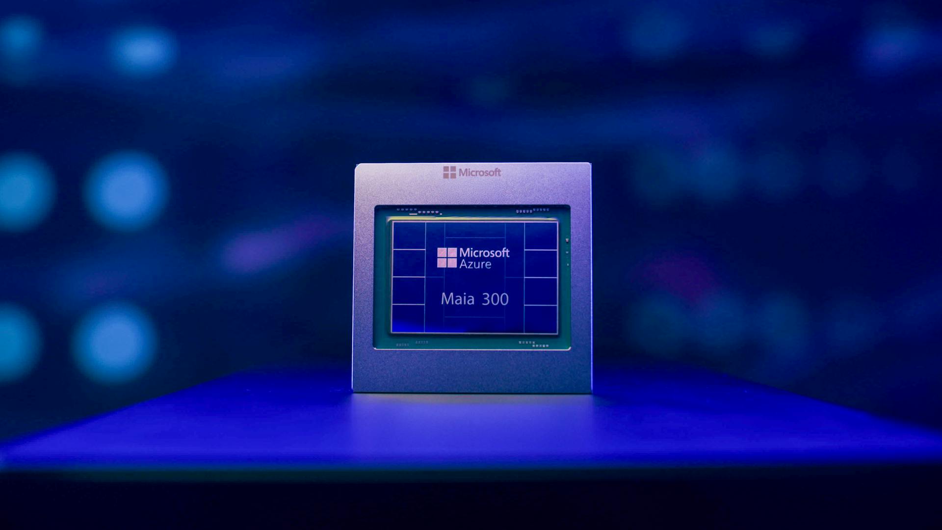
Microsoft is doubling down on the AI chip race once again. Its next-generation AI inference platform, Maia 300, has officially been unveiled, with a clear positioning — targeting long-context reasoning, low-latency conversation, and agent scenarios, and claiming it will support Azure's multi-gigawatt-scale inference deployments.
Maia 300's Core Specifications
Based on officially disclosed information, Maia 300 brings several key hardware upgrades:
- 8 HBM4 memory stacks: Compared to the previous generation, the higher-bandwidth memory subsystem directly serves long-context scenarios, eliminating the need for models to frequently shuttle data between VRAM and external storage.
- TSMC N2P process compute chiplets: Leveraging an advanced process node to gain an edge in energy efficiency.
- 96-accelerator racks: Using whole racks as deployment units, pointing toward hyperscale clusters rather than single-card shipments.
Microsoft's key metric is a 40% increase in token throughput per megawatt of power consumption. This figure is worth noting — it's not about single-chip peak compute, but rather "performance per watt," indicating that Maia 300's design focus is on the economics of large-scale inference.
HBM4 (High Bandwidth Memory 4) is the fourth-generation high-bandwidth memory standard led by JEDEC. By vertically stacking multiple layers of DRAM dies and interconnecting them with compute chiplets via a silicon interposer, it achieves bandwidth and energy efficiency far beyond traditional GDDR. Compared to HBM3E, HBM4 expands the interface width from 1024 bits to 2048 bits, with single-stack bandwidth capable of exceeding 2TB/s, while reducing energy consumption per bit at the same capacity. For long-context inference, the KV cache (key-value cache) expands linearly with sequence length, and memory bandwidth often becomes the bottleneck before compute — this is precisely why Microsoft emphasizes "8 HBM4 stacks": more stacks mean greater capacity and wider bandwidth channels, thereby reducing the overhead of model weights and KV cache traveling to and from external storage.
N2P is a performance-enhanced version within TSMC's 2nm family, a derivative process following its N2 node. N2 introduced Gate-All-Around (GAA) nanosheet transistors for the first time, replacing the FinFET structure, achieving higher drive current at the same power consumption, or reducing leakage and power consumption at the same frequency. N2P further optimizes on this basis, typically providing a few percentage points to about a ten percent improvement in performance or energy efficiency. For AI accelerators, advanced process nodes are not just about peak compute — they directly impact performance per watt, which is precisely the underlying support Maia 300 relies on when highlighting "token throughput per megawatt."
Chiplet refers to splitting what was originally a single large chip into multiple functional modules, each manufactured using the most suitable process, then integrated onto the same substrate through advanced packaging (such as CoWoS or similar 2.5D/3D packaging). The benefits: compute logic uses the most advanced node to ensure energy efficiency, while I/O or cache portions can use mature nodes to reduce cost and risk, while also improving yield. Maia 300 states that its compute portion uses N2P chiplets, meaning Microsoft is pursuing energy efficiency while also using a chiplet strategy to control the usage and manufacturing complexity of advanced process nodes.
Why "Inference" Rather Than Training?
This generation of Maia has a clear positioning: an inference platform. Microsoft emphasized in its announcement that it targets three types of workloads — long-context reasoning, low-latency conversation, and agents — and these three directions happen to correspond to the most compute-intensive parts of Microsoft's current product lineup.
Long-context reasoning means models need to process longer inputs; low-latency conversation requires first-token response to be fast enough; and agents require frequent, multi-round tool calls and reasoning loops. Combined, these three place far greater pressure on inference infrastructure than traditional single-turn Q&A.
Making inference the main battleground also aligns with Microsoft's business logic. Training can be concentrated in a few supercomputing clusters, but inference is an ongoing cost that occurs every day, for every user, on every request. Whoever can lower the per-token cost of inference can take the initiative in AI product margins.
Long-context reasoning refers to models needing to process inputs of tens of thousands to millions of tokens, such as entire documents, code repositories, or multi-turn conversation histories. The challenge is not just that attention computation grows quadratically with sequence length, but also the large amount of VRAM consumed by the KV cache and the resulting bandwidth pressure. Low-latency conversation focuses on time-to-first-token (TTFT) and inter-token output intervals, directly determining users' perception of chat products. Agents involve letting models autonomously plan, call tools, and execute tasks in multi-round loops — a single user request may trigger dozens of model calls, multiplying the demands on inference throughput and scheduling efficiency. What these three workload types share is extreme sensitivity to memory bandwidth, interconnect latency, and performance per watt, rather than simply pursuing peak floating-point performance during training. This also explains why dedicated inference chips tend to focus on the memory subsystem and rack-level interconnect rather than simply stacking compute.
What Multi-Gigawatt Means
"Multi-gigawatts" is the most significant statement in this announcement. It elevates the discussion from "how many cards were deployed" to "how much electricity is being consumed."
A gigawatt-scale data center is an energy infrastructure-level existence. Microsoft stated that Azure Maia will scale to multi-gigawatt deployments and become the primary inference system for Microsoft's own products. In other words, Maia 300 is not just an optional cloud accelerator, but will gradually replace the third-party chips that Microsoft's internal inference workloads depend on.
This also explains why Microsoft is building its custom chips in whole-rack form — at multi-gigawatt scale, network topology, power delivery, and cooling design matter more than single-chip metrics.
Gigawatt-scale data centers typically refer to facilities with sustained power delivery capacity reaching 1GW (approximately 1 million kilowatts), equivalent to the output of a large nuclear power unit or several gas power plants. Currently, the world's largest AI training clusters mostly consume hundreds of megawatts, and "multi-gigawatt" means Microsoft is planning inference infrastructure several times that scale. At this scale, power acquisition, substation connections, cooling (liquid cooling or immersion), and network cabling become primary constraints, while single-chip peak metrics take a back seat. This is also the fundamental reason cloud providers are shifting to whole-rack delivery: rack-level design can unify power buses, liquid cooling loops, and high-speed interconnect topologies, standardizing deployment and operations to support scale expansion.
Production Timeline and Rollout Schedule
The announcement mentions that production will begin in 2027. The long window between announcement and mass production aligns with the realistic cycle for advanced process and HBM4 capacity ramp-up. For Microsoft, this time is also used for software stack adaptation — whether the chip can reach full utilization depends on the maturity of compilers, operator libraries, and framework support.
The Next Step in the Custom Chip Race
Microsoft is not the only cloud provider betting on custom AI chips. The arrival of Maia 300 makes the "cloud providers building custom inference chips" path even clearer: no longer pursuing general-purpose compute, but designing customized solutions for their own models and product forms.
The 40% token-per-megawatt improvement is a strong selling point, but it remains Microsoft's own figure for now. The real test will be whether Maia 300, after mass production in 2027, can deliver on its multi-gigawatt deployment promise with stable yields and a usable software ecosystem.
One-line Summary
Microsoft unveils Maia 300 inference chip, targeting multi-gigawatt Azure deployments and per-watt performance advantages.
Paragraph Summary
Microsoft has officially unveiled its next-generation AI inference platform, Maia 300, positioned for long-context reasoning, low-latency conversation, and agent scenarios. On the hardware side, it features 8 HBM4 memory stacks, TSMC N2P compute chiplets, and a 96-accelerator rack form factor, with the company claiming a 40% increase in token throughput per megawatt of power consumption. The chip will support Azure's multi-gigawatt inference deployments and gradually become the primary inference system for Microsoft's own products. Production is planned to begin in 2027, at which point it will serve as an important test of the cloud providers' custom inference chip path.
Related articles

JobRunner MCP Server: AI Agents Can Now Fix Failed Java Jobs
JobRunner launches an open-source MCP server enabling AI agents to view cluster status, diagnose failures, and recover Java jobs—incident response from any cloud coding environment or existing agent.

MLAI Digital Launches 9 Security Agents: MCP Server Safeguards the Full Lifecycle of Agentic AI
MLAI Digital launches Security MCP Server with nine built-in specialized security agents covering vulnerability discovery, attack simulation, prompt injection detection, API and infrastructure assessment, and accelerated remediation—embedding security validation across the full Agentic AI lifecycle from development to production.

Running Isaac Lab on H100 GPUs: Exploring Better Approaches
Exploring optimization methods for running Isaac Lab on NVIDIA H100 GPUs, including MIG configuration, mixed precision, TensorRT acceleration, and community experience to improve robotics simulation and reinforcement learning efficiency.