PCB Art Badges: When Alchemical Symbols Meet Circuit Board Design

How makers transform PCBs into alchemical art badges using circuit board manufacturing techniques.
This article explores the intersection of PCB manufacturing and alchemical-cosmological art, showing how creators use solder mask, silkscreen, exposed copper, and board cutouts to craft wearable badges that blend medieval mystical symbols with modern electronics. It covers the complete workflow from concept to prototype, the tools and techniques involved, and the cultural significance of this growing maker movement.
When Circuit Boards Meet Alchemy
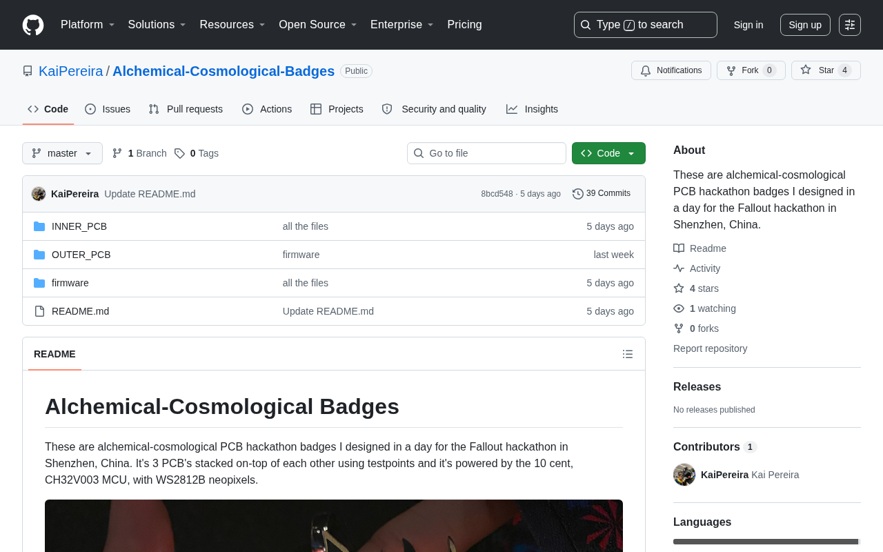
In the world of hardware geeks, PCBs (Printed Circuit Boards) have long ceased to be merely functional substrates for electronic components — they're gradually evolving into a unique medium for artistic expression. Recently, a creator shared their project on Hacker News: a series of PCB badges featuring alchemical-cosmological themes, capturing the attention of the hardware community.
This type of project falls within the increasingly popular "PCB Art" category in the maker community. Creators combine traditional printed circuit board manufacturing processes with visual elements from mysticism, astronomical symbols, and alchemical icons to produce physical works that blend technical sophistication with cultural aesthetics.
What Are PCB Badges
PCB badges are typically small, wearable circuit board creations. They may be purely decorative, or they might incorporate LED lighting effects, microcontrollers, or even simple interactive features. At various tech conferences (such as DEF CON, hackathons worldwide), custom badges have long served as social currency and identity symbols, with attendees trading and collecting these exquisite electronic badges.
DEF CON is the world's largest hacker and information security conference, founded in 1993 and held annually in Las Vegas. Its official badge adopted the electronic PCB format starting in 2006, with increasing complexity each year — evolving from simple LED blinking to complete computing systems featuring wireless communication, cryptographic challenges, and even running Linux. This spawned a thriving unofficial badge ecosystem known as the "badgelife" community. Participants design, manufacture, and sell or give away custom badges, forming a unique geek social culture. A typical high-end DIY badge might feature an ESP32 or STM32 microcontroller, OLED display, accelerometer, and interconnect with other badges via the SAO (Shitty Add-On) standard interface. This culture has expanded to tech conferences worldwide, becoming an important vehicle for the open-source hardware community to express creativity and identity.
What makes this particular project special is its thematic choice — alchemy and cosmology. This combination juxtaposes medieval mystical symbol systems with modern electronic manufacturing processes, creating a striking temporal tension.
The Collision of Alchemical Aesthetics and PCB Manufacturing
Alchemical symbols — such as the three-element icons representing mercury, sulfur, and salt, along with astronomical markers for the sun, moon, and planets — are inherently highly graphic and symmetrical, making them perfectly suited for translation into silkscreen patterns and copper trace artwork on circuit boards.
To understand why these symbols are so well-suited to the PCB medium, we need to trace their historical context. Alchemy originated in the Egyptian-Greek tradition of antiquity, was transmitted through the Arab world into medieval Europe, and developed into a complete symbolic language system. Its core theory revolves around the philosophy that "all things can be transformed," positing that through specific operations (such as the seven great processes of calcination, distillation, sublimation, etc.), material purification and transcendence can be achieved. The alchemical symbol system includes elemental symbols (such as an inverted triangle representing water, an upright triangle representing fire), planetary-metal correspondences (gold corresponds to the Sun, silver to the Moon, copper to Venus, etc.), and philosophical icons (such as the Ouroboros representing eternal cycles, the hexagram representing the unity of opposing forces). On the cosmological side, ancient cosmic models like Ptolemy's geocentric system also produced abundant geometricized visual expressions, including concentric celestial sphere diagrams and zodiac symbols. The common characteristics of these symbols are their high degree of geometrization, strong symmetry, and rich philosophical metaphor, making them naturally suitable as visual design elements on circuit boards.
In PCB manufacturing, creators can deploy multiple "layers" as artistic brushes:
- Solder mask: Commonly green, but customizable in black, white, red, purple, blue, and other colors to form the background tone;
- Silkscreen: Typically white text and patterns, used for drawing fine lines;
- Exposed copper: Gold-plated or tin-plated copper surfaces exhibit metallic luster, useful for highlighting areas;
- Cutouts: Through irregular board cuts, giving badges unique non-rectangular outlines.
From a manufacturing perspective, PCB production is based on a subtractive process: a photosensitive dry film is applied to a copper-clad laminate (typically FR-4 fiberglass epoxy resin substrate), the design pattern is transferred to the copper surface through exposure and development, then etchant removes unwanted copper foil, with the remaining copper forming circuit traces or artistic patterns. The solder mask is an epoxy resin coating applied after etching to protect the copper and prevent short circuits during soldering. For artistic PCBs, the ENIG (Electroless Nickel Immersion Gold) process is particularly popular because it creates a flat, oxidation-resistant gold surface on exposed copper, with visual results far superior to standard HASL (Hot Air Solder Leveling) tin surfaces.
Alchemical and cosmological themes happen to fully leverage these process characteristics — golden exposed copper perfectly presents the "philosopher's stone" gold imagery, while dark solder mask creates a mysterious, profound cosmic backdrop.
PCB Art Creation: A Cross-Disciplinary Skill Worth Exploring
From a technical perspective, creating such a badge requires spanning multiple knowledge domains. Creators must not only master EDA (Electronic Design Automation) tools like KiCad or Eagle, but also understand PCB manufacturing process constraints while possessing graphic design aesthetic sensibility.
EDA tools were originally designed for circuit engineers, but PCB artists have developed a unique workflow. KiCad is currently the most popular open-source EDA software, created by CERN's Jean-Pierre Charras in 1992, and after over thirty years of development now offers complete schematic editing and PCB layout capabilities. In artistic creation, designers typically complete vector graphic design in Inkscape or Adobe Illustrator, then convert SVG files to KiCad's footprint format through the svg2shenzhen plugin (an image import tool developed specifically for KiCad), automatically assigning them to corresponding PCB layers. The commercial tool Eagle (now part of Autodesk Fusion Electronics) similarly supports comparable import workflows. Key technical constraints include: minimum silkscreen line width typically of 0.15mm, and minimum copper clearance depending on manufacturing capability (typically 0.1-0.15mm). These limitations directly affect pattern detail and force creators to fully consider manufacturing feasibility during the design phase.
The PCB Badge Creation Workflow
Behind a seemingly simple artistic badge typically lies this process:
- Concept and reference gathering: Establishing the alchemical and cosmological symbol systems and visual style;
- Vector graphic conversion: Converting symbolic patterns into vector files suitable for various PCB layers;
- Layer mapping: Deciding which elements to render in copper foil, silkscreen, or solder mask;
- Electrical design (optional): If LEDs or chips are included, actual circuit routing must be completed;
- Prototyping and iteration: Small-batch prototyping to verify results, with repeated adjustments to colors and process parameters.
Since PCB colors and materials are difficult to fully preview in design software, physical prototypes often reveal unexpected differences in effect — this is what makes PCB art creation both challenging and deeply captivating.
The Cultural Significance of Hardware Creation
The value of such projects extends far beyond "making a good-looking circuit board." It represents a movement within open-source hardware culture that re-imbues functional industrial products with humanistic and artistic value.
As the marginal cost of industrial manufacturing has dramatically decreased with the proliferation of PCB prototyping services (today, prototyping a dozen small PCBs costs just a few dollars), individual creators have gained unprecedented freedom of expression. This cost revolution is inseparable from the maturation of the PCB supply chain in Shenzhen, China: prototyping services like JLCPCB and PCBWay have driven the price of five 100×100mm double-layer PCBs down to $2-5 (excluding shipping), with lead times shortened to within 24 hours. Before the 2010s, equivalent prototyping typically started at hundreds of dollars with lead times of several weeks. This "two-dollar board" model allows individual creators to experiment with PCB designs as casually as printing photos. Meanwhile, services like OSH Park (USA) offer high-quality boards with purple solder mask, and manufacturers like Elecrow support over a dozen solder mask color options, providing a rich "palette" for artistic creation. The proliferation of SMT assembly services further lowers the barrier for producing badges with electronic components.
Creators can use circuit boards as a creative medium just as artists use canvas, exploring the intersection of technology and aesthetics.
The theme of alchemy itself carries apt metaphorical weight — ancient alchemists attempted to transmute base metals into gold, while modern hardware creators use gold-plated copper foil and precision manufacturing to "transmute" ordinary fiberglass substrates into artworks that combine function with beauty. This resonance between ancient and modern is what makes this project most thought-provoking.
How to Start Your PCB Art Journey
Although this project attracted limited attention during its initial release, the maker spirit and cross-disciplinary creative philosophy it reflects are worth noting. In an era where AI and software dominate the tech discourse, this kind of hardware work that "tells stories with hands and circuit boards" reminds us that technological creation can equally be filled with poetry and humanistic concern.
For interested readers, consider getting started with PCB design using open-source tools like KiCad, beginning with a small artistic badge to experience the joy of transforming ideas into physical objects. The recommended entry path is: first complete KiCad's official tutorial to familiarize yourself with basic operations, then try drawing simple graphics in Inkscape and importing them via the svg2shenzhen plugin, and select low-cost prototyping services like JLCPCB or OSH Park for your first physical verification. The entire process from zero to receiving your first finished badge typically takes only one to two weeks and less than ten dollars in cost.
Key Takeaways
Related articles

Workbuddy for Absolute Beginners: How a Desktop AI Agent Fits Into Real Workflows
A beginner's guide to the Workbuddy desktop AI agent: installation, claiming credits, file management, and building automated workflows—compared with CodeX for fit and cost, helping professionals shift from AI question-askers to AI managers.

OpenAI's New Agent Stack: Computer Use, Decisions API, and Ultra-Fast Workflows
OpenAI Dev Day unveiled a new agent stack: Computer Use outperforms humans, Decisions API delivers ultra-low-latency classification via Luna, Agents API opens the same Computer Use capabilities, and GPT-6.1 Sol costs only one-seventh of Astra. Core updates, benchmark data, and developer insights.

Liang Wenfeng Open-Sources DeepInfo Inference Framework, Takes On U.S. Ban
DeepSeek open-sources its DeepInfo inference framework after its models, featuring GPU/CPU cross-pipelining, small-model prediction with large-model verification, and full Huawei Ascend and NVIDIA chip support—facing the U.S. federal ban head-on. This article analyzes its significance for AI deployment and open-source strategy.