Why Chip Manufacturing Is Nearly Impossible: The Truth About ASML and TSMC's Global Collaboration

Moore's Law is a collective self-fulfilling prophecy; the chip industry is hard to replicate.
Based on Gideon Lewis-Kraus's visits to ASML and TSMC, the article reveals that Moore's Law is not a physical law but a collective pre-commitment mechanism across the supply chain—each company promises to build equipment that doesn't yet exist. EUV lithography, reliant on Zeiss mirrors of atomic precision, is the most irreplaceable step, with only ASML able to build it. TSMC cleanrooms are 1,000x cleaner than operating rooms, and wafers travel the equivalent of New York to Taiwan daily. Chipmaking spans dozens of countries and thousands of firms, depending on 40 years of tacit knowledge; localization is a generational project. No one fully understands an ASML machine—knowledge dispersion is both vulnerability and moat.
Moore's Law Is Not a Law of Physics, but a Collective Self-Fulfilling Prophecy
Most people take it for granted that chip performance doubles every two years—it seems like inevitable technological progress. But《The New Yorker》writer Gideon Lewis-Kraus, sharing his reporting experience on The Vergecast, completely overturns this narrative of "inevitability." After visiting ASML and TSMC, his core conclusion is: nothing about progress in the chip industry is "a given"—it is more like a carefully orchestrated collective illusion that ultimately became a self-fulfilling prophecy.
A senior physicist at ASML told Lewis-Kraus bluntly: "Moore's Law? I don't care at all. That's for people who haven't actually done this work—it's just marketing." The implication is that frontline engineers never work to a "double every two years" timetable; they face the hard constraints of physical laws. What truly keeps Moore's Law alive is a "pre-commitment mechanism" among companies across the supply chain—when drawing up roadmaps for the next fifteen years, each company commits to building equipment that doesn't yet exist and may never be achievable, on the condition that suppliers make the same commitment.
This mechanism sounds almost reckless, yet it constitutes the most fundamental collaborative logic of the chip industry. According to Lewis-Kraus's observations, participants at many stages don't even think much about end-customer demand; what matters more to them is "not letting down their partners' expectations." This sports-like motivation for research—purely to challenge "what no one has done before"—has instead become the invisible engine of the industry's continuous breakthroughs.
Lithography Machines: The Most Irreplaceable Diamond in the Crown of Human Industry
To understand the difficulty of chip manufacturing, lithography is the best entry point. Lewis-Kraus summarizes this step as "painting with light": projecting chip design patterns onto silicon wafers to etch circuit architectures. As transistor density increases, light sources with ever-shorter wavelengths are needed—like carving extremely fine patterns with an ever-sharper scalpel.
The problem is that light wavelengths have physical limits. As early as the early 1990s, the entire industry realized that continuing with existing light sources would eventually hit a dead end. So Intel took the lead, with assistance from the U.S. government, and joined with industry to launch a long-term plan to find alternatives. After fifteen to twenty-five years of effort, what finally landed was extreme ultraviolet lithography (EUV)—and only one company in the world, ASML, can build such machines.
The irreplaceability of EUV machines manifests on two levels. First, without the lithography step there are no chips, and without ASML's EUV equipment there are no advanced-process chips. Second, even if chips can be "printed," they must achieve throughput of hundreds of wafers per hour to be cost-effective. According to information Lewis-Kraus cited on the program, China has made progress in deep ultraviolet lithography (DUV, the previous generation technology), but prototype equipment capacity is about thirty to fifty wafers per hour—still a considerable distance from commercial cost-effectiveness.
ASML's lithography machines also rely on mirrors manufactured by Germany's Zeiss. These mirrors are made of forty alternating layers of carbon and molybdenum, each deposited almost atom by atom, with a manufacturing cycle of up to two years and costs in the millions of dollars. Lewis-Kraus used a stunning analogy to describe their flatness: if a mirror were scaled up to the size of a world map, the highest variation would be equivalent to the thickness of a playing card lying flat on the ground. Another set of mirrors' precision was described as "being able to precisely hit one side of a coin from the Moon."
Extreme Ultraviolet Lithography (EUV) is the most advanced chip lithography technology today, using extreme ultraviolet light with a wavelength of 13.5 nanometers. This wavelength is so short that it is absorbed by almost all materials, including air and glass, so the entire optical path must propagate in a vacuum, and lenses are replaced by multilayer mirrors coated with alternating molybdenum and silicon to focus the light. For the light source, ASML uses lasers to hit tin droplets to generate plasma that excites extreme ultraviolet light—this process occurs tens of thousands of times per second, placing extremely high demands on stability and precision. EUV technology took nearly twenty years to develop, involving coordinated breakthroughs in optics, materials, plasma physics, and other fields, and is the key enabling technology for chip processes entering nodes below 7 nanometers.
Deep Ultraviolet Lithography (DUV) is the mainstream lithography technology before EUV, mainly using argon fluoride (ArF) excimer lasers with a wavelength of 193 nanometers. Because of the longer wavelength, DUV requires immersion lithography (adding deionized water between the lens and the wafer) and multiple patterning techniques to improve resolution when manufacturing smaller feature sizes. DUV equipment can cover needs from mature processes to some advanced processes, and is currently the workhorse equipment for many chip manufacturing steps. Compared with EUV, DUV technology is mature and lower-cost, but faces physical limits at nodes below 7 nanometers and must rely on EUV to achieve smaller transistor densities.
Inside a Chip Factory: A Thousand Times Cleaner Than a Hospital Operating Room, Wafers Travel "New York to Taiwan" Daily
Lewis-Kraus gained a rare opportunity to enter a TSMC factory. Before entering the cleanroom, he had to put on full protective gear, could not carry any metal objects, and then underwent static testing and an air shower. The cleanroom was extremely quiet, with floor tiles covered in ventilation holes, and the entire space's atmosphere was completely replaced at regular intervals. For technical reasons, lighting was yellow, and combined with the low hum of the ventilation system, he described the feeling as "being in London during the Blitz, but everything spotless."
How clean is it? He specifically verified a figure: measured in parts per million of impurity particles in the air, the cleanroom is about a thousand times cleaner than a hospital operating room—not a vague rhetorical flourish, but a fact backed by clear metrics.
The level of automation inside the factory is equally stunning. Miles of track networks are mounted overhead, with mechanical grippers resembling arcade game claws speeding along the tracks, grabbing specialized containers holding wafers, delivering them to one end of equipment and retrieving them from the other. According to Lewis-Kraus, a single wafer travels a distance within a single factory in one day equivalent to a round trip from New York to Taiwan. The factory he visited had a cleanroom area large enough to hold twenty-two standard football fields simultaneously—and this was just one of TSMC's dozens of factories. After the tour, a TSMC employee checked step-count data on an Apple Watch—they had walked about five miles indoors.

Cleanrooms are the core environment of chip manufacturing, graded by the number of particles greater than or equal to 0.5 micrometers per cubic foot of air. An ISO Class 1 cleanroom requires no more than 10 particles larger than 0.1 micrometers per cubic meter of air, while hospital operating rooms are typically ISO Class 7 or lower. TSMC's advanced-process cleanrooms achieve ISO Class 1-3, thousands of times cleaner than operating rooms. To maintain this environment, cleanrooms use laminar airflow, high-efficiency air filters (HEPA/ULPA), and positive pressure control; personnel must wear full-body protective suits, with even breath and skin flakes strictly isolated. In addition, yellow lighting is used to prevent photoresist from being accidentally exposed during non-exposure steps.
Why Can't the Chip Industry Be "Moved Back to America"?
In recent years the United States has pushed for localization of chip manufacturing, but Lewis-Kraus's reporting reveals an easily overlooked fact: chips are not "manufactured" in one place—they cross national borders dozens of times and involve thousands of companies.
The supply chain's starting point is already highly geographically constrained. The high-purity quartz crucibles needed to make silicon ingots come from raw materials sourced from the world's only high-purity quartz mine, in the mountains of western North Carolina. Polysilicon purification is concentrated among three companies, located in Michigan, Germany, and Japan respectively. After that, almost every step relies on a small number of highly specialized suppliers, forming what Lewis-Kraus calls a "global superorganism"—it exists simultaneously all over the world and cannot simply be cut apart and relocated.
More critical is tacit knowledge. Chip manufacturing relies on an engineering community that has accumulated over forty years, with established training institutions, tight personal networks, and a great deal of experience that is difficult to document. When TSMC built its factory in Arizona, even the cleaning of cleanroom protective suits could not be done locally—they had to search across the desert for a suitable laundry service. This may seem like a small problem, but it reflects the absence of an entire supporting ecosystem.

However, Lewis-Kraus also recorded a perspective that surprised him. Mike Schmidt, who led the implementation team for the Biden administration's chips act, responded to the criticism that "TSMC can't even wash protective suits" by saying: this precisely means someone will build a cleanroom laundry. He emphasized that this plan was never something that could be completed within one election cycle, but was planned on a thirty-to-forty-year scale—just as Morris Chang knew when he founded TSMC in 1987 that this was a generational project.
This leads to a deep contradiction: the global division of labor in the chip industry is both the most successful exemplar of globalization and the most fragile node in geopolitics. Lewis-Kraus believes two paths can proceed in parallel—gradually increasing distributed layout of capacity while respecting the balance of the existing industrial ecosystem. He warns that simply "correcting" this market from the perspective of economics textbooks and pursuing a more fully competitive equilibrium could instead destroy the entire system. The deep collaborative relationship between ASML and Zeiss, where "you can't tell who works for whom," is precisely where efficiency cannot be measured by traditional market models.
Tacit Knowledge refers to experiential knowledge that is difficult to transmit through text, documentation, or standardized processes; it exists in engineers' intuition, operational skills, and collaborative conventions. Chip manufacturing involves thousands of process steps, and many parameter adjustments and troubleshooting rely on long-accumulated "feel" and on-site judgment rather than manuals. For example, the assembly and adjustment of lithography machine lenses, the cleaning cycles of etch chambers, and the rapid attribution of wafer defects all require experienced engineering teams to make on-site decisions. This knowledge is dispersed across a global engineering community formed over forty years and is difficult to replicate or transfer quickly, becoming the biggest soft barrier to localizing chip manufacturing.
No One Truly Understands the Whole Machine
Near the end of the interview, host David Pierce asked a fundamental question: does anyone fully understand how chips are made? Lewis-Kraus's answer was no. Not only laypeople—even physicists on ASML's light source team cannot fully explain how other modules on the same machine work. "No single person truly understands the entirety of an ASML machine, let alone the entire industry."
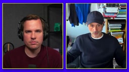
But this is precisely where the value of Lewis-Kraus's reporting lies. He admits he is a "professional dabbler" who cannot possess true technical depth, but he is capable of answering the most basic question: why can't chip manufacturing just "build a factory and be done"? After completing this journey, his feeling was—"Oh, now I understand why it's so hard."
This cognitive gap can also be summed up with one detail. In the late 1970s, Gordon Moore remarked: if other industries could progress at the same rate, we would drive at 100,000 miles per hour, get 50,000 miles per gallon, and cars would be so cheap you could throw away a Rolls-Royce and buy another to drive home. This analogy seems almost absurd today, but Lewis-Kraus points to an everyday example: a digital pregnancy test, used and discarded by countless people every day, has far more computing power than the navigation computer of the Apollo lunar module—and it only needs to display a plus or minus sign. The wonder of the chip industry is hidden in this thoroughly normalized miracle.
One-line Summary
Moore's Law is a self-fulfilling prophecy of collective pre-commitment; the chip industry is hard to replicate.
Paragraph Summary
Based on Gideon Lewis-Kraus's visits to ASML and TSMC, the article reveals that Moore's Law is not a law of physics but a collective pre-commitment mechanism among companies across the supply chain—each commits to building equipment that doesn't yet exist, driving continuous breakthroughs. EUV lithography machines are the most irreplaceable link in chip manufacturing, relying on Zeiss mirrors of atomic precision, and only ASML can build them. TSMC's cleanrooms are a thousand times cleaner than operating rooms, and a wafer's daily travel equals a New York–Taiwan round trip. Chip manufacturing spans dozens of countries and thousands of companies, relying on forty years of tacit knowledge; localization is a generational project measured in decades. No one fully understands an ASML machine, and the dispersion of knowledge is both a vulnerability and a moat.
Related articles

GPT-6.2 Astra and Sol Released: Dual-Model Architecture and Community Buzz
OpenAI releases GPT-6.2 with Astra and Sol models. This article summarizes the official announcement and Hacker News discussion, analyzing the potential impact of the dual-model architecture on developers and offering selection advice.

Gmod TTT Egyptian-Themed Map: Space Capitalism vs. the Pharaoh
Explore the fun of a Gmod TTT Egyptian-themed map: players pick roles like pharaoh, teleport to space via a cube, and engage in a humorous capitalism vs. communism showdown with chaotic prop fighting.

GraphRAG: Beyond Search, Toward Global Knowledge Discovery
GraphRAG is a knowledge-graph-enhanced retrieval technology from Microsoft Research that goes beyond local search in traditional RAG to enable global knowledge discovery. This article introduces its core ideas, generational evolution, and healthcare use cases.