Can AI Design Circuit Boards? A Deep Dive into the Realities and Limitations of AI in PCB Design
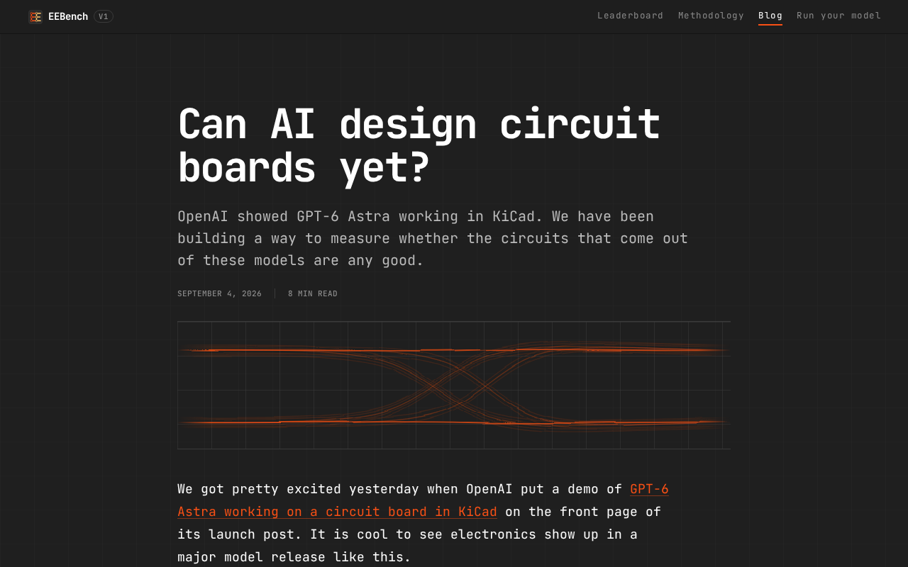
AI can assist with PCB design tasks but cannot yet independently design circuit boards.
This article examines whether AI can design circuit boards by analyzing its current capabilities and limitations in PCB design. While AI excels at component selection, datasheet lookup, and EDA scripting, it falls short in physical layout and routing due to expensive feedback loops, scarce training data, and the tacit engineering knowledge required. The most promising path forward is AI-augmented EDA tools that combine pattern recognition with precise constraint solving.
A Tempting Question: Can AI Design Circuit Boards?
Now that large language models can write code, generate images, and assist with research, hardware engineers naturally ask: can AI actually design circuit boards (PCBs)? This question recently sparked a lively discussion on Hacker News, earning 113 upvotes and nearly 70 comments. The answer is more complex than you might expect — AI's performance in circuit design offers both exciting breakthroughs and deep-seated limitations.
PCB (Printed Circuit Board) design is a highly specialized engineering task involving schematic design, component selection, layout and routing, signal integrity analysis, power distribution, thermal management, and more. The full PCB design workflow typically spans several phases: first comes schematic design, where engineers use EDA tools to draw out the logical connections of a circuit, defining the electrical relationships between components; next is component selection, choosing specific parts based on electrical parameters, package dimensions, availability, and cost; then comes the most critical phase — layout and routing, which maps the logical connections from the schematic into physical space, determining where each component sits on the board and how traces are routed; finally, design verification is needed, including signal integrity simulation, thermal simulation, and manufacturability reviews. Unlike writing software, hardware design mistakes often translate into real financial losses — a single PCB prototype run can cost hundreds of dollars, and if it involves ASIC tape-out, costs can easily reach tens of thousands or even millions of dollars, plus weeks or months of lead time. This makes the question "Can AI handle PCB design?" especially worth examining carefully.
What AI Can Actually Do in Circuit Board Design
Based on community discussions, current AI tools demonstrate practical value in supporting roles within circuit design, but remain far from "end-to-end autonomous design."
Applications Already in Practice
Large language models can provide tangible help to hardware engineers in several areas:
- Component selection and datasheet lookup: Recommending suitable chips, resistors, capacitors, and other components based on design requirements, and quickly retrieving key parameters from datasheets — saving engineers enormous amounts of time spent poring over documentation. Electronic component datasheets typically run dozens or even hundreds of pages, packed with electrical characteristics, recommended operating conditions, package dimensions, and typical application circuits. A single major chip manufacturer (such as TI or ADI) may have tens of thousands of part numbers in its catalog, and engineers must compare parameters across massive volumes of documentation during the selection phase — precisely the kind of information retrieval and summarization task that LLMs excel at.
- Schematic logic assistance: Helping engineers understand how a particular circuit block works, or providing typical reference designs to accelerate design decisions. Reference designs are recommended circuit solutions provided by chip manufacturers in datasheets or evaluation board documentation. These are thoroughly validated and serve as important starting points for new designs. AI can quickly locate and explain these reference designs, helping engineers understand the design intent and the rationale behind key parameter choices.
- EDA scripting and automation code generation: For EDA tools that support scripted operations like KiCad, AI can generate automation scripts that dramatically speed up repetitive tasks. EDA (Electronic Design Automation) is the core toolchain for hardware design. The current EDA market has a clear tiered structure: the commercial end is dominated by three giants — Cadence Allegro, Synopsys, and Mentor Graphics (now Siemens EDA) — whose tools hold absolute dominance in high-end chip and complex PCB design; the mid-market features tools like Altium Designer targeting small and medium enterprises; and the open-source space is led by KiCad, which has developed rapidly in recent years and can now handle quite complex PCB projects. KiCad supports a Python scripting interface that allows engineers to programmatically control schematic editing, PCB layout, BOM (Bill of Materials) generation, and more — enabling AI-generated automation scripts to plug directly into workflows, automating previously tedious operations like batch component placement and bulk parameter modifications.
- Design documentation and compliance checking: Reviewing design documents and flagging potential compliance issues.
The common thread across these scenarios is that AI plays the role of a "knowledge assistant" rather than a "design decision-maker." It accelerates information retrieval and repetitive labor, but the core engineering judgment remains firmly in human hands.
PCB Layout and Routing: The Enormous Gap AI Faces
The real challenge lies in physical layout and routing. This is the most experience-intensive phase of PCB design, requiring engineers to simultaneously balance electrical performance, manufacturing processes, cost, form factor, and other competing constraints. Many seasoned hardware engineers in the community pointed out that AI's current performance in this area is far from usable — generated layouts frequently violate basic electrical rules or produce designs that are physically impossible to manufacture.
It's worth noting that auto-routing is not a new concept; traditional EDA tools have long included algorithmic auto-routers. Auto-routing technology dates back to the 1960s, with early approaches using the Lee algorithm (a maze-routing algorithm based on breadth-first search) and the A search algorithm*, later evolving into channel-assignment-based routing methods and more modern constraint-driven routing engines. Commercial auto-routers like Cadence's PCB Router and Altium's ActiveRoute are quite mature, capable of handling connections across thousands of nets. Yet even these tools, refined over many years, often fall short when faced with complex high-speed circuits. High-speed digital circuits (such as DDR4/DDR5 memory interfaces, PCIe buses, and high-speed serial links) impose extremely strict requirements on trace length matching, impedance control, and crosstalk isolation — requirements that auto-routers often cannot satisfy, which is why professional engineers tend to trust the quality of manual routing. For AI to achieve a breakthrough here, it needs not just language understanding capabilities, but deep modeling of physical-world constraints.
Why Circuit Board Design Is Harder for AI to Crack Than Writing Code
The Fundamental Absence of a Feedback Loop
Software development has an enormous structural advantage: feedback is nearly instantaneous and free. When code is wrong, the compiler throws an error, execution crashes, and developers can iterate within seconds. This rapid feedback mechanism is also a key factor behind the rapid improvement of AI coding capabilities — models like AlphaCode and Codex can generate millions of candidate solutions and quickly filter them through automated testing, with each failure serving as an inexpensive learning signal. Hardware design verification, by contrast, is extremely costly — you need to actually manufacture the circuit board (PCB prototyping typically takes 3–7 days, or 24–48 hours for expedited runs), solder components (hand-soldering a moderately complex board can take several hours), power it up, and test it before you know whether the design actually works. Even simulation tools (such as SPICE circuit simulation or Ansys HFSS electromagnetic simulation) can only verify certain characteristics, and setting up simulations itself requires considerable expertise.
This expensive feedback loop means that training AI for circuit design suffers from a severe lack of the massive, cheap trial-and-error data available in software. Publicly available PCB design datasets are also far scarcer than code datasets — GitHub hosts billions of lines of open-source code, while publicly available PCB projects with complete design files and verification results are comparatively rare. AI cannot "fail fast and learn fast" the way it can when debugging code, which fundamentally constrains the pace of model improvement.
Tacit Knowledge and Engineering Intuition Resist Digitization
Circuit design is steeped in the tacit knowledge of experienced engineers: how to arrange decoupling capacitors for effective filtering, how to handle ground planes to reduce noise, how to avoid electromagnetic interference (EMI), how to prevent signal reflection — much of this knowledge has never been fully documented and instead resides in the experience and intuition engineers have accumulated over many years. AI struggles to adequately learn this kind of deep knowledge from publicly available text.
Take Signal Integrity (SI) as an example: when high-speed signals travel along PCB traces, the trace is no longer a simple wire but a transmission line with characteristic impedance. If the transmission line's impedance doesn't match the driving or receiving end, signals will reflect, causing waveform distortion and timing errors. To control impedance, engineers must precisely calculate trace width, distance to the reference plane, the dielectric constant of the PCB substrate, and other parameters — calculations that rely on simplified models of Maxwell's equations. Closely related is Power Integrity (PI): when chips switch at high speeds, they generate transient current demands. If the power distribution network (PDN) is poorly designed, voltage fluctuations result (known as "ground bounce" and "power droop"), which in turn degrade signal quality. Decoupling capacitor selection and placement exist precisely to provide a low-impedance transient current path near the chip. Additionally, Electromagnetic Compatibility (EMC/EMI) requirements demand that designs meet radiation and conducted emission limits set by international certification standards such as FCC and CE — involving grounding strategies, shielding design, filter circuits, and an entire system of engineering practices.
More critically, a circuit is a system strictly governed by the laws of physics. Maxwell's equations, thermodynamic laws, and material properties all silently constrain the design space. Current large language models are fundamentally text sequence predictors (autoregressive or encoder-decoder models based on the Transformer architecture) that generate plausible-looking text through statistical pattern matching, but lack causal understanding of the physical world. An LLM might "know" that decoupling capacitors should be placed close to the chip, but it doesn't understand that the reason is to minimize parasitic inductance and thereby reduce PDN impedance — this absence of physical causal reasoning makes it prone to "confidently hallucinating" in scenarios requiring rigorous physics-based reasoning, generating solutions that sound professionally worded but actually violate physical laws.
A Pragmatic Path: Collaboration Between AI and Hardware Engineers
Synthesizing the community discussion, a pragmatic consensus is emerging: In the near term, AI will not replace hardware engineers, but will become a powerful collaborative tool.
The more likely development path is a combination of "specialized tools + AI augmentation" rather than general-purpose LLMs going it alone. Embedding AI capabilities into mature EDA workflows — such as intelligent Design Rule Checking (DRC), layout suggestions based on historical design data, and natural language-driven parameter configuration — these incremental improvements are more realistic and commercially valuable than "having AI design an entire circuit board from scratch."
Design Rule Check (DRC) is a critical quality gate in the PCB design process. Traditional DRC operates on deterministic rules: checking whether trace spacing meets minimum clearance requirements, whether via sizes conform to manufacturer specifications, whether copper-to-board-edge distances are sufficient — these are precisely quantifiable geometric constraints. But in real engineering practice, there are also many "soft rules" and context-dependent best practices, such as "high-speed differential pairs should not have parallel single-ended traces nearby" or "sensitive analog signal areas should be kept away from switching power supply circuits." AI-enhanced DRC has the potential to bring these hard-to-codify experiential insights into the checking process, learning what "good design looks like" by analyzing large numbers of historical design cases, thereby catching potential design risks at an early stage.
Several startups and open-source projects are actively exploring this direction. For example, Quilter AI is attempting to use AI for automated PCB layout and routing, combining reinforcement learning with constraint optimization to handle complex physical constraints; Flux AI is trying to build an AI-assisted browser-based PCB design tool to lower the barrier to entry for hardware design; academic research teams are exploring the use of Graph Neural Networks (GNNs) to model circuit netlists, leveraging the natural graph structure of circuits to predict design quality metrics. Among the EDA giants, Cadence and Synopsys are also integrating machine learning capabilities into their respective toolchains — for example, using ML models to accelerate simulation convergence and optimize the search space for layout solutions. This hybrid architecture, combining AI's pattern recognition abilities with the precise constraint-solving capabilities of traditional EDA tools, complementing AI's strengths with the rigor of engineering tools, may well be the right approach to intelligent hardware design.
Conclusion: The Current State and Future Outlook of AI-Assisted PCB Design
Returning to the original question: "Can AI design circuit boards now?" The answer is: it can assist, but it cannot yet design independently. In areas like component selection, knowledge retrieval, and script generation, AI is already a practical and efficient assistant; but in layout, routing, and physical verification — where real engineering judgment is tested — it still has a long way to go before replacing human engineers.
The unique characteristics of hardware design — high verification costs, extensive tacit engineering knowledge, and strict physical constraints — ensure that it won't be disrupted by AI as quickly as software development. From a technological development perspective, breakthroughs may come from several directions: first, advances in hardware simulation technology that make virtual verification more accurate and affordable, thereby providing AI with faster feedback loops; second, the emergence of specialized foundation models — domain-specific models pre-trained on large volumes of circuit design data that may understand the inherent patterns of hardware design better than general-purpose LLMs; and third, the development of multimodal AI that can simultaneously process the visual information of schematics and PCB layouts alongside text descriptions, forming a more complete understanding of the design. But all of these advances will take time.
For hardware engineers, rather than worrying about being replaced, it's better to think about how to leverage AI tools to amplify your own productivity. Hand off the repetitive labor to AI and keep the engineering judgment for yourself — that is perhaps the most rational and pragmatic attitude for the present moment.
Related articles
Vercel AI SDK TUI: A New Option for Terminal-Based AI Interaction
Vercel AI SDK introduces @ai-sdk/tui for terminal AI interactions, bringing streaming output, tool calling, and AI conversations to the command line.
Microsoft Copilot Copyright Lawsuit: 8.2 Million Conversations Reveal the Truth About AI Content Copying
Microsoft discloses 8.2M Copilot conversations in NYT copyright lawsuit, claiming AI rarely copies news content. Explore the key data, legal disputes, and implications for the AI industry.

HydraFusion Explained: How GitHub Copilot's Multi-Model Orchestration Cuts Costs by 67%
Deep dive into GitHub Copilot's HydraFusion multi-model orchestration: its Plan-Build-Critique-Complete workflow, how it cuts costs by 67%, and the paradigm shift from model selection to orchestration.