Did AI Really Design OpenTPU? A Sober Look at This Open-Source Project

OpenTPU is a promising full-stack open-source TPU demo, but its "AI-designed chip" claim lacks transparency and verifiable evidence.
OpenTPU is an open-source hardware project that packages RTL, an instruction set, a simulator, a compiler, and a profiler in a single repository — and went viral after being labeled "AI designing an AI chip." In reality, it runs on a Kintex 7 FPGA rather than taped-out silicon, barely meets timing at 133 MHz, is limited to small models like LFM 2.5 230M (59–85.8 tokens/sec), and quickly hits DDR3 memory bandwidth limits. Most critically, the README discloses nothing about how AI and human engineers divided the design work, making the "AI-autonomous" narrative unverifiable. OpenTPU represents genuine early exploration at the AI-hardware intersection, and its open toolchain has reference value — but it falls far short of proving that AI can autonomously iterate and optimize chip design.
An open-source project called OpenTPU has been generating buzz — largely because it's been described as "AI designing its own AI chip." The claim attracted widespread attention, but strip away the hype and look at the technical details, and this looks more like an encouraging proof-of-concept than a genuine case of "chip self-evolution."
What the Project Actually Delivers
OpenTPU's most appealing trait is its completeness: the entire tech stack lives in a single repository, including RTL (Register Transfer Level descriptions), an instruction set, a simulator, a compiler, and even a profiler. For an open-source hardware project, this "full-stack in one repo" approach meaningfully lowers the barrier for understanding and reproducing the work — which is part of why it went viral so quickly.
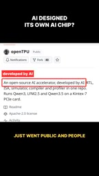
One thing worth clarifying upfront: this is not a taped-out chip. It runs on a Kintex 7 FPGA development board, which means it emulates the hardware design through programmable logic arrays rather than manufacturing an actual ASIC. That distinction matters enormously — FPGA validation is an early stage in the chip design process, and there's a long road between here and production silicon.
A quick primer on the terminology: RTL (Register Transfer Level) is a key abstraction layer in chip design that describes how data flows between registers and the corresponding logic operations. Designers write RTL in hardware description languages like Verilog or VHDL; the code then goes through synthesis, place & route, and other steps before producing a manufacturable layout file (GDS). An FPGA is a reprogrammable chip composed of configurable logic cells and interconnects that can emulate a given RTL design's behavior. An ASIC (Application-Specific Integrated Circuit) is a custom chip that has actually been fabricated in a foundry and permanently etched into silicon. The core difference: FPGA validation can be completed in hours and modified at will, but its performance and power efficiency are nowhere near final silicon. ASIC tape-out takes months, costs millions of dollars, and achieves frequencies and energy efficiency that FPGAs simply can't match. The gap between "running on an FPGA" and "building a chip" spans the entire industrial chip design pipeline.
Performance: Viable for Small Models, but Clearly Constrained
Looking at the measured data, OpenTPU's timing is quite tight — it barely meets timing closure at 133 MHz. That's not a high clock frequency for a modern inference accelerator, and it signals that the design is still in a very early stage of refinement.

On the inference side, it achieves roughly 59 tokens/sec running the LFM 2.5 230M model, rising to 85.8 tokens/sec with 4-bit quantization; another set of figures shows a related model dropping from 30.6 to 21.6. Across the board, these numbers only apply to very small models, and performance quickly hits the DDR3 memory bandwidth ceiling.
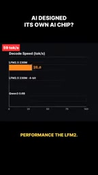
In other words, the bottleneck isn't just the compute units themselves — it's data movement. Memory bandwidth limitation is a classic problem for inference accelerators, and OpenTPU's constraints here directly dictate that it can currently only serve lightweight models. Running mainstream large models is a distant prospect.
On memory bandwidth bottlenecks: This is a central challenge in neural network inference accelerator design. The industry typically uses arithmetic intensity (floating-point operations per byte of memory access) to gauge whether a model or operator is bandwidth-bound. The autoregressive decoding phase of large language models is a classic memory-bound workload — generating each token requires reading nearly the full set of model weights, while the actual compute is relatively modest. DDR3's theoretical bandwidth sits in the 10–25 GB/s range, while the HBM (High Bandwidth Memory) found in Google's TPU v4 or NVIDIA's H100 can exceed 800 GB/s — a 30× difference. This means that no matter how capable OpenTPU's compute units become, as long as the memory interface stays at DDR3, there's an inescapable bandwidth ceiling. Larger models simply cannot run efficiently under these constraints.
Does the "AI-Designed Chip" Claim Hold Up?
This is the part of the project most worth scrutinizing. The project's README doesn't explain how much work humans versus AI contributed at each stage of the design process, or how responsibilities were divided. Without that critical information, the "AI autonomously designed this chip" narrative has no verifiable foundation.

Chip design is a highly complex systems engineering discipline. From architecture definition to timing closure, every step can involve extensive human intervention. If AI only assisted at certain points — say, generating portions of the RTL code or offering optimization suggestions — that's an entirely different claim from "AI independently designed a chip." Without a transparent account of the workflow, calling this a "self-improvement loop" is premature at best.
On the current state of AI-assisted chip design: The mainstream application of AI in EDA (Electronic Design Automation) today involves using large language models or reinforcement learning for specific sub-tasks within the design flow — for example, using LLMs to generate and debug RTL code snippets, using reinforcement learning to optimize floorplanning (Google's 2021 Nature paper on chip floorplanning is the canonical example), and using machine learning to accelerate simulation or timing analysis. These approaches have meaningfully improved efficiency at specific steps, but the overall design flow still depends heavily on human engineers for architectural decisions, verification strategy, and final sign-off. There is currently no industry-recognized complete case of "AI autonomously completing the full chip design flow" — it remains largely in the realm of academic exploration. Evaluating whether a project has truly achieved "AI-designed chips" hinges on whether it can provide complete, reproducible workflow logs that clearly attribute each design decision to a human or a model. That transparency is precisely what OpenTPU currently lacks.
How to Think About This Project Rationally
To be fair, OpenTPU does represent a genuine step forward in the direction of AI participation in chip design. Open-sourcing the complete toolchain so that more people can participate, scrutinize, and improve the work has real value in itself.
But the hype calls for some level-headedness: this is currently a demonstration project running on an FPGA, limited to small models, constrained by memory bandwidth, and opaque about its division of labor. It proves out a possibility — it does not prove the grand claim that "AI can autonomously iterate and design better chips."
For developers and researchers interested in the intersection of AI and hardware, the more pragmatic approach is to treat OpenTPU as an early-stage specimen worth studying — paying attention to its toolchain design philosophy and open-source ecosystem, rather than being swept up in "AI builds chips" headlines. Real breakthroughs will require more transparent evidence and more mature engineering execution.
Related articles

Amphibious Transforming Drone: Beyond 100x Power Savings, What Are the Real Needs?
Is the amphibious transforming drone just a gimmick? Starting from the 100x power difference of the M4 Morphobot, explore real application scenarios and thesis topic ideas, analyzing boundary conditions where pure drones and pure ground robots both fail.

Warhound Raises $200 Million: Genetically Engineered "War Dogs" Paired with Anduril Gear
Warhound raises $200M, backed by Ben Lamm and Palmer Luckey, to genetically engineer dogs for military and law enforcement use and equip them with Anduril gear. This article analyzes its technology direction, funding logic, and ethical controversy.

Claude API Comes to Google Cloud: IAM Integration and SDK Access Guide
Anthropic hosts the full Claude API on Google Cloud with IAM-controlled permissions and unified billing. This guide covers the Vertex AI and Anthropic-hosted entry points, IAM role configuration, and SDK access.