Micron's $10 Billion R&D Center in Boise: A Deep Dive into Its Strategic Significance
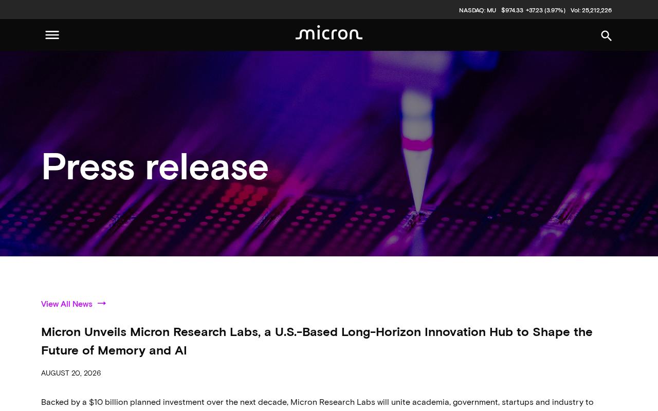
Micron invests $10B in a Boise R&D center to advance HBM and next-gen memory for the AI era.
Micron Technology is investing $10 billion to build a major R&D center at its Boise, Idaho headquarters, targeting breakthroughs in HBM and next-generation memory technologies critical to AI. Fueled by the CHIPS and Science Act and supply chain security concerns, the investment complements Micron's $100B+ New York fab and aims to close the gap with Samsung and SK hynix in the high-bandwidth memory market driving AI computing.
Micron's $10 Billion Bet: Why Boise?
Global memory chip giant Micron Technology has announced a massive investment of up to $10 billion to establish a large-scale R&D center in Boise, Idaho — the city where the company is headquartered. This represents one of the largest single domestic investments in Micron's history and marks yet another significant move in the semiconductor industry amid the backdrop of geopolitical tensions and supply chain restructuring.
Boise holds profound significance for Micron. The company was founded in 1978 by Ward Parkinson, Joe Parkinson, Dennis Wilson, and Doug Pitman in the basement of a dental office in Boise. Over more than four decades, it has grown into the world's fourth-largest semiconductor company by revenue and one of the top three memory chip manufacturers globally, with fiscal year 2024 revenue exceeding $25 billion. As the company's birthplace and global headquarters, Boise carries the weight of Micron's historical roots. Concentrating tens of billions of dollars in R&D resources at its home base is both a renewed bet on domestic manufacturing and innovation capabilities, and a clear signal: in the fiercely competitive memory chip arena, R&D innovation will be the core variable that determines who wins and who loses.
Strategic Positioning in the Wave of Semiconductor Reshoring
Micron's massive investment is not an isolated event — it's part of the broader trend of semiconductor industry reshoring in the United States. Since the passage of the CHIPS and Science Act, semiconductor companies including Intel, TSMC, and Samsung have all ramped up factory construction and R&D spending on American soil.
Driven by Policy Incentives and Industrial Security
The CHIPS and Science Act was signed into law by President Biden in August 2022, with a total authorization of approximately $280 billion. Of that, roughly $52.7 billion is earmarked directly for semiconductor manufacturing and R&D, including $39 billion in manufacturing subsidies and $13.2 billion for R&D and workforce development. The act also provides approximately $24 billion in tax credits applicable to semiconductor manufacturing equipment investments. Its core objective is to reverse the decline of America's share of global chip manufacturing — from 37% in 1990 to approximately 12% in 2020 — and rebuild domestic semiconductor manufacturing and R&D capabilities. Notably, the act includes "guardrail provisions" that prohibit companies receiving subsidies from making significant advanced-node expansions in countries of concern, including China, for a period of 10 years.
Behind this wave of investment lies the combined force of policy incentives and industrial security considerations. Tax breaks and subsidies from federal and state governments have significantly lowered the cost barrier for domestic expansion, while the chip shortage during the pandemic gave major manufacturers a visceral understanding of the risks of over-reliance on overseas supply chains. Consolidating R&D and manufacturing operations domestically has become a strategic consensus for ensuring supply chain resilience.
For Micron specifically, being the only major memory chip manufacturer headquartered in the United States gives its domestic R&D strengthening a unique strategic value. In the DRAM and NAND flash markets, Micron faces intense competition from Korean giants Samsung and SK hynix, and the intensity of R&D investment directly determines its voice in next-generation memory technologies. To elaborate: DRAM (Dynamic Random Access Memory) is a volatile memory — data is lost when power is cut — primarily used as main memory in computers and servers, characterized by extremely fast read/write speeds. NAND flash, on the other hand, is non-volatile memory widely used in solid-state drives, smartphone storage, and similar applications. The industry-leading 3D NAND technology has now achieved vertical stacking of over 200 layers. In the global memory market, Micron, Samsung, and SK hynix collectively hold approximately 95% of the global DRAM market share, making it a highly concentrated competitive landscape.
The Industrial Significance of an R&D Center: Why Not a Fab?
Here's a noteworthy detail: Micron chose to invest in an R&D center rather than simply a wafer fabrication plant (fab). This positioning deserves careful consideration. In the semiconductor industry, manufacturing capacity is certainly important, but what truly determines long-term competitiveness is often cutting-edge technology R&D capability.
In the semiconductor industry, fabs and R&D centers serve fundamentally different roles. Fabs focus on high-volume mass production, with a single advanced-node fab typically requiring investments of $10 billion to $20 billion or more, with costs concentrated on lithography equipment (such as ASML's EUV — extreme ultraviolet — lithography machines, priced at over $300 million each), etching equipment, deposition equipment, and other manufacturing tools. R&D centers, by contrast, focus on frontier innovation activities such as new material exploration, new architecture design, process node development, and product prototype validation. It's worth noting that Micron is simultaneously investing over $100 billion in a large-scale fab in Clay, New York — one of the largest single private investments in U.S. history — and the Boise R&D center and the New York manufacturing base form a complementary "R&D + Manufacturing" framework. The new processes and design solutions produced by the R&D center ultimately need to be brought to mass production through fabs — both are indispensable.
Racing to Dominate Next-Generation Memory Technologies Like HBM
As artificial intelligence, data centers, and high-performance computing place unprecedented demands on memory bandwidth and capacity, new memory products such as High Bandwidth Memory (HBM) are becoming an industry focal point. HBM is a memory solution that uses advanced packaging technology to vertically stack multiple layers of DRAM chips and interconnect them closely with GPU/AI accelerator chips through a silicon interposer. Compared to traditional DDR memory, HBM achieves bandwidth improvements of several times — even more than tenfold — through thousands of parallel data channels. The latest generation, HBM3E, can include 8 to 12 DRAM dies in a single stack, delivering bandwidth exceeding 1TB/s.
The explosive growth of AI large models has directly driven demand for high-performance memory. Training and inference for large language models require reading and writing massive parameter data in extremely short timeframes, and the bandwidth bottleneck of traditional memory severely constrains the computational power of AI accelerators — this is precisely why HBM has become a critical component of the AI era. NVIDIA's H100, H200, and B200 GPUs all rely heavily on HBM. Currently, SK hynix holds approximately 50% of the HBM market, Samsung about 40%, and Micron roughly 10%. However, Micron's HBM3E products have demonstrated outstanding energy efficiency and have already received NVIDIA certification. Whoever achieves breakthroughs first in HBM, next-generation DRAM, and other technologies will secure an advantageous position in the AI-era chip race.
The $10 billion R&D investment is Micron's concrete commitment to betting on this future. By building a powerful R&D cluster at its headquarters, Micron aims to integrate resources more efficiently, accelerate the transition of new technologies from lab to mass production, and narrow the gap with competitors on the critical HBM battlefield.
Far-Reaching Impact on Boise's Regional Economy
For Boise and the entire state of Idaho, this investment will generate significant economic multiplier effects. Large R&D centers typically create numerous high-paying technical positions, attract top engineering and research talent, and in turn catalyze the growth of surrounding supporting industries and service sectors.
This "anchor effect" is particularly pronounced in the semiconductor industry. The anchor effect is an important concept in regional economics, referring to how a large core enterprise can act like an "anchor" that fixes an entire industrial chain in a specific region. The establishment of a core R&D center often drives the collaborative clustering of upstream and downstream suppliers, equipment manufacturers, and even university research institutions, gradually forming a regional technology innovation ecosystem. The cluster effect in semiconductors is especially typical: an R&D center requires the support of specialty gas suppliers, ultrapure water treatment companies, precision instrument maintenance service providers, EDA (Electronic Design Automation) tool companies, IP licensing firms, and a large pool of specialized talent.
Take the Portland metropolitan area in Oregon as an example: after Intel established a factory there in 1974, it gradually attracted hundreds of semiconductor-related companies to cluster in the area, forming a tech hub known as the "Silicon Forest." Boise already has a certain foundation in the semiconductor industry — besides Micron, companies such as HP and ON Semiconductor also have R&D or manufacturing facilities in the area. This multi-billion-dollar investment is poised to accelerate Boise's transformation from a "single-company-dominated" economy to a "diversified industrial ecosystem." Additionally, Idaho's relatively lower cost of living and tax burden, compared to traditional tech hubs like Silicon Valley and Seattle, offers a differentiated appeal for talent. For regions hoping to build emerging tech centers outside the traditional Silicon Valley model, Boise's case offers valuable lessons.
Conclusion: A Strategic Bet on the Future of Memory Chips
Micron's $10 billion R&D center investment is both a commitment to its domestic roots and a forward-looking positioning for future technology trends. At a time of profound restructuring in the semiconductor industry landscape, this decision reflects a renewed recognition of the value of R&D innovation and strategic positioning on the eve of an AI-driven explosion in memory demand.
The actual results of this multi-billion-dollar investment will still take time to materialize — whether the R&D center can be completed on schedule and whether it can incubate technologically competitive market outcomes will be the ultimate measures of this investment's value. But Micron's move has already provided a highly significant case study for observing the trajectory of the U.S. semiconductor industry and the competitive landscape of memory chips.
Related articles

Complete Guide to Deploying Large Models Locally with Ollama: From Installation to Code Integration
Complete guide to deploying large models locally with Ollama, including custom installation paths to avoid C drive issues, practical commands, and LangChain integration code examples for building offline private AI development environments.

Canada Declares Trade War with the United States: Impact Analysis and Outlook
Canada's PM declares the country is in a trade war with the U.S. — a historic escalation. We analyze impacts on supply chains, tech, AI talent, and more.

AI Won't Replace Senior Developers — It Will Push Their Value Upstream
Will AI replace programmers? From radiologists to coachmen, learn how AI pushes developer value upstream. Master architecture, judgment, and skills AI can't replace.