TSMC A14 Process Node Revealed: A New Breakthrough in Next-Gen Chip Manufacturing
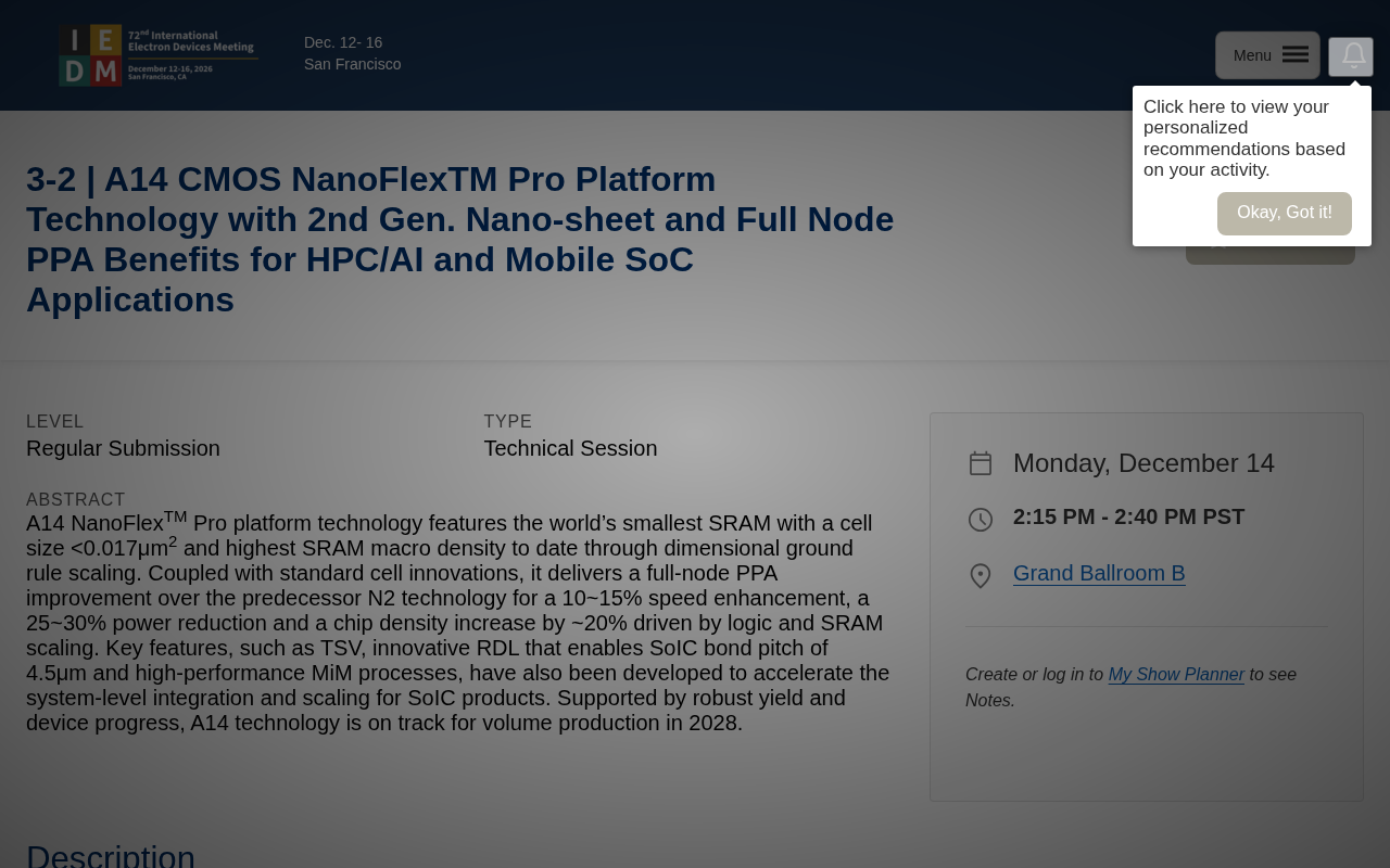
TSMC unveils A14 (1.4nm) node details, officially marking the chip industry's entry into the angstrom era.
TSMC has disclosed technical details on its next-generation A14 process node. Using the angstrom naming convention, A14 corresponds to roughly 1.4nm and is a key step beyond N2 on the advanced process roadmap. The node is expected to build on GAA nanosheet transistor architecture to tackle leakage and performance challenges at extreme scales, while requiring costly cutting-edge equipment like High-NA EUV. Surging AI compute demand has intensified pressure from major customers like NVIDIA and Apple for more advanced nodes, making A14 capacity highly coveted. Meanwhile, competitive pressure from Samsung and Intel has prompted TSMC to signal its continued technology leadership through roadmap disclosures.
TSMC Discloses New Details on the A14 Node
TSMC, the world's largest contract chipmaker, has recently disclosed some technical details about its next-generation A14 process node. As a pivotal step on the semiconductor roadmap, A14 represents TSMC's major push into the 1.4-nanometer scale — what the industry is calling the "angstrom era." The announcement has sparked considerable discussion in the tech community, reflecting the industry's keen interest in where advanced process technology is headed.
In terms of naming, TSMC has been gradually transitioning from the traditional "nanometer" convention to a system using "A" (for Angstrom). The "14" in A14 corresponds to 14 angstroms, roughly equivalent to 1.4 nanometers, marking yet another step toward the physical limits of transistor scaling.
Note: Given the limited information in the original source material (a brief Hacker News entry), this article provides context and analysis on the A14 node's technical background and industry significance. Specific specifications should be verified against TSMC's official announcements.
Why the A14 Node Matters
Continuing the Process Roadmap
TSMC's process roadmap has advanced from N5 (5nm) and N3 (3nm) through to N2 (2nm), with A14 representing the next generation beyond N2. Each new node brings higher transistor density, improved power efficiency, and performance gains — all of which directly impact the competitiveness of high-end chips for smartphones, data centers, AI accelerators, and more.
Driven by AI Compute Demand
As the demand for compute power for large model training and inference grows explosively, chipmakers face unprecedented pressure to adopt ever more advanced process nodes. Smaller transistors mean more compute units per unit area and lower power consumption — critical factors for AI data centers that consume enormous amounts of electricity. If A14 enters volume production on schedule, it will become a highly sought-after capacity resource for major customers like NVIDIA, Apple, and AMD.
Technical Challenges of the Angstrom Era
Evolution of Transistor Architecture
At such microscopic scales, traditional FinFET architecture can no longer keep up. The industry has broadly shifted to GAA (Gate-All-Around) transistors to control leakage and improve performance. TSMC began introducing nanosheet technology at the N2 node, and A14 is expected to further refine this approach to achieve a better balance between gate control and current drive capability.
The fundamental difference between GAA and the previously dominant FinFET architecture lies in how the gate wraps around the channel. In FinFET, the gate surrounds a fin-shaped silicon structure on three sides, whereas GAA fully wraps the gate around nanosheets or nanowires on all four sides, dramatically improving channel current control and suppressing short-channel effects and leakage. Nanosheet technology is a specific implementation of GAA that horizontally stacks multiple thin silicon layers to increase current drive capability while maintaining a small footprint. Samsung was first to volume-produce GAA at its 3nm node, while TSMC chose to introduce it at N2, calling it the "Nanosheet FET." At the A14 stage, fine-tuning parameters such as the number of stacked nanosheet layers, sheet thickness, and spacing will directly determine the final performance and power characteristics.
Lithography and Manufacturing Costs
Advancing to the angstrom scale requires cutting-edge equipment such as High-NA EUV (High Numerical Aperture Extreme Ultraviolet) lithography. These machines come with enormous price tags, and as process complexity increases, the R&D and production costs for advanced nodes continue to rise. Managing yield while controlling costs is a shared challenge for both TSMC and its customers.
High-NA EUV is the current frontier of lithography technology, developed and manufactured by ASML. Compared to existing EUV tools with a numerical aperture of 0.33, High-NA raises the NA to 0.55, improving theoretical resolution by approximately 40%. This enables finer patterning in a single exposure, reducing the number of multi-patterning steps and thus improving efficiency while lowering alignment errors. However, a single High-NA EUV machine costs approximately $350–400 million — more than double the price of existing EUV tools — and its massive size places extremely high demands on fab infrastructure. TSMC has already procured High-NA EUV equipment for R&D purposes, but whether full-scale deployment can be achieved during volume production will directly affect wafer costs and yield ramp speed for the A14 node.
The Competitive Landscape
TSMC has long maintained a lead in advanced process technology, but Samsung and Intel are actively working to close the gap. Samsung is betting on GAA to leapfrog the competition, while Intel is restructuring through its foundry business in an attempt to re-enter the top tier of the process race. The disclosure of A14 technical details is, in some sense, TSMC's way of signaling to the market and its customers that its roadmap is advancing steadily — reinforcing its authority in the high-end foundry market.
Conclusion and Outlook
The unveiling of the A14 node once again confirms that semiconductor process technology continues its steady march toward physical limits. While the details disclosed so far are incomplete, they sketch the technical contours of the next generation of advanced chips. For readers tracking AI hardware, consumer electronics, and the semiconductor industry, the A14 production timeline, real-world power efficiency, and the first products to adopt it will all be worth following closely.
As more official information is released, the market will ultimately answer just how significant a performance and efficiency leap the A14 node will deliver.
Related articles
Free DeepSeek V4.1 Flash via DSH: Bulk Point Collection & International WorkBuddy Tested
DSH project update tested: WorkBuddy now offers 100 points per claim, rate limits raised beyond 80M tokens with faster resets, and international WorkBuddy supports free Hunyuan 4 and DeepSeek V4.1 Flash.

Capsule: Pack Web Apps and Data into a Single SQLite File
Capsule is a Rust/Tauri 2.0 tool that packs HTML web apps and data into a single SQLite file — privacy-first, local storage, portable sharing, with AI support.

DSH-SUBAGENT-UI Plugin: The Ultimate Sub-Agent Manager for DeepSeek Harness
DSH-SUBAGENT-UI is a DeepSeek Harness browser plugin offering sub-agent overview, search, local categorization, and completion snapshots — install with one command.