OpenAI's 13-Month Jalapeño Chip: Can It Really Crush NVIDIA?

OpenAI's 13-month Jalapeño ASIC beats Blackwell on select benchmarks, but selective data and ASIC trade-offs warrant caution.
OpenAI launched its in-house Jalapeño chip project in October 2024 and taped it out at TSMC just 13 months later. The ASIC draws ~700W while delivering nearly 3× the memory capacity of the H100 and 15.4 TB/s of HBM4 bandwidth, achieving up to 9× the throughput of competing solutions on an 8K 1K inference benchmark. However, OpenAI published only a single benchmark scenario, omitting agentic workload tests like AgentX. Its scale-up bandwidth of 600 GB/s per GPU trails NVIDIA NVL72's 900 GB/s, though a global scale-out topology connecting up to 16 racks compensates. The chip already runs GPT-OSS, DeepSeek R1, and Kimi K2.5, and OpenAI is using its own models to accelerate kernel development. With second and third generations already in development, AI's iteration race has officially reached the chip layer.
OpenAI kicked off its in-house chip project, codenamed Jalapeño, in October 2024 — and just 13 months later, the first design was already being taped out at TSMC. The lab best known for its models and AI agents has suddenly unveiled a chip that's challenging NVIDIA's Blackwell on inference tasks, turning heads across the entire industry. But when you dig into the early benchmark data and technical details, the story turns out to be far more nuanced than any "crushing NVIDIA" headline would suggest.
How Impressive Are Jalapeño's Numbers on Paper?
Jalapeño's early benchmarks paint an aggressively optimistic picture. Serving Kimi K2.5 at 100 tokens/sec, it delivers nearly 9× the throughput of the second-place contender, with peak throughput reaching 700 tokens/sec. Running the GPT-OSS 120B model, that peak climbs to 1,500 tokens/sec — roughly double the next best option.
What's even more noteworthy is its power profile. Jalapeño draws around 700W, comparable to the H100 and H200, yet packs nearly 3× the memory capacity of the H100 and roughly 5× the bandwidth. Compared to Blackwell, it consumes half the power at similar memory capacity while delivering twice the bandwidth — backed by HBM4 memory providing 15.4 TB/s of bandwidth.

This combination of low power, high bandwidth, and large memory capacity isn't accidental. OpenAI's monthly active users have surpassed 1 billion — equivalent to serving 13% of the global population — making data center power supply a real bottleneck. Rather than brute-forcing through the energy layer, the strategy is to build a more power-efficient custom chip: do more with less electricity. That's the core design motivation behind Jalapeño.
General-Purpose Chips vs. ASICs: Two Very Different Paths
The key to understanding Jalapeño is recognizing that it and NVIDIA are walking entirely different roads. NVIDIA builds general-purpose chips that handle both training and inference across a wide range of use cases. OpenAI is building an ASIC — an Application-Specific Integrated Circuit — that is ruthlessly optimized for a very narrow set of tasks.
This distinction shows up directly in raw compute. At FP8 precision, Jalapeño delivers roughly 3.4 petaflops — higher than the H100 and H200, but noticeably behind Blackwell, and far below the upcoming Rubin generation. In other words, on raw compute alone, Jalapeño doesn't win.
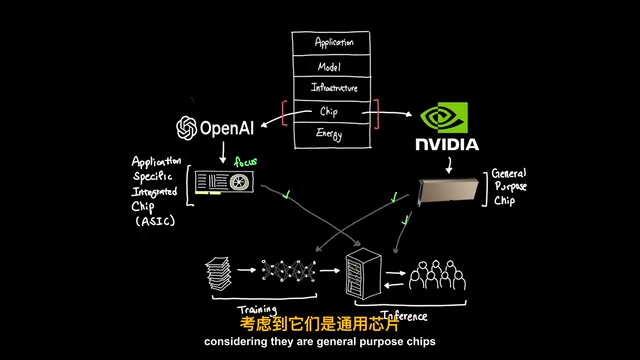
OpenAI's trade-off is deliberate: forget being all-things-to-all-workloads; just make inference fast and power-efficient. Inference itself breaks down into two phases — pre-fill and decode. The decode phase is bandwidth-bound, while pre-fill depends on compute and memory capacity. Jalapeño puts its resources squarely on bandwidth and memory, targeting exactly where large-scale inference services actually hit their limits.
What is an ASIC? An ASIC (Application-Specific Integrated Circuit) is a chip custom-built from the ground up for a specific workload. Compared to a general-purpose GPU, it can strip away all the logic units that aren't needed for its target task, redirecting that saved die area and power budget entirely toward its intended use case. Google's TPU was one of the earliest ASICs to achieve large-scale deployment in AI, designed specifically for the matrix-multiplication-heavy workloads of neural network training and inference. Amazon's Trainium/Inferentia and Meta's MTIA follow the same philosophy. The trade-off is flexibility: once a chip is taped out — meaning the design is sent to a fab for manufacturing — its circuit structure is frozen. Any new operators or precision formats outside the original design assumptions may require significant software-level workarounds, or simply wait for the next hardware generation. This is why ASIC vendors typically extract maximum value only after model architectures have stabilized — betting on the wrong architecture carries enormous consequences.
A Benchmark That Was Carefully Curated
Behind those impressive numbers lies a detail worth scrutinizing. The benchmark OpenAI published is labeled "8K 1K" — a single entry from the open-source test suite InferenceX, simulating a scenario with 8,000 input tokens and 1,000 output tokens. The problem: OpenAI only released this one data point.
The tests that truly stress-test a chip's limits are suites like AgentX — which measures chip performance in agentic scenarios involving heavy back-and-forth calls, long contexts, and long-running sessions that more closely reflect real-world usage. Those numbers haven't been made public.
A reasonable inference is that OpenAI may not yet have fully tuned the chip and its configuration for scenarios beyond 8K 1K. The early numbers are genuinely impressive, but Jalapeño's consistency across diverse inference tasks remains unproven. Treating a single-slice benchmark as evidence that "NVIDIA is dethroned" is clearly premature.
ASICs also carry an inherent risk that general-purpose chips don't: they must make much bolder assumptions about upstream requirements. If a fundamentally new model architecture emerges, or the way agentic applications call models changes at a foundational level, it's this highly customized chip that takes the hit.
What does "8K 1K" mean? This notation describes the input/output token ratio in LLM inference: 8,000 input tokens (prompt length) against 1,000 output tokens (generated response length). This ratio has a decisive effect on how workload pressure is distributed across an inference chip — longer inputs intensify pre-fill phase demands on compute and memory access, while output token count directly determines how long the decode phase runs. Real-world token distributions vary enormously: a simple Q&A might involve just a few hundred input tokens, while an agent executing a multi-step task could have an input context exceeding 100,000 tokens with thousands of output steps. Test suites like AgentX are designed specifically to simulate these multi-turn, long-context, high-concurrency agentic workloads. A single 8K 1K data point only reflects throughput at one specific input/output ratio — it cannot represent a chip's aggregate performance across the full distribution of inference tasks.
Scale-Up vs. Scale-Out: The Infrastructure Battle
Models like DeepSeekAd R1 and Kimi K2.5 simply don't fit on a single chip — they require scale-up (inter-chip communication within a rack) and scale-out (interconnecting multiple racks into a cluster) to stack compute. This is where different vendors show their hand.
NVIDIA uses NVL72: two Blackwell GPUs paired with a Grace CPU per module, connected via NVLink C2C, with 72 GPUs per rack stitched together into one logical machine via NVLink and NVSwitch, delivering 900 GB/s per GPU.
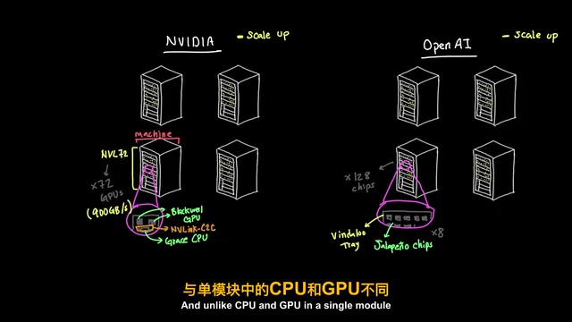
OpenAI takes a different approach: 8 Jalapeño chips per Vindaloo tray, 16 trays per rack for 128 chips total. Rather than co-locating CPU and GPU in the same module like NVIDIA, it places CPUs in a separate Katsu tray connected via switches. This configuration delivers 600 GB/s per GPU — roughly 66% slower than NVL72's scale-up bandwidth.
On the scale-out side, NVIDIA uses InfiniBand through external switches to connect multiple racks. Jalapeño takes a "global scale-up" approach, connecting up to 16 racks at 200 GB/s in what's described as a cubic 3D topology — a design philosophy that bears a resemblance to Google's TPU interconnect strategy.
Scale-Up vs. Scale-Out Explained Scale-up and scale-out represent two fundamentally different expansion strategies in distributed computing. Scale-up means adding more chips within a single node or rack and connecting them with high-speed interconnects (like NVLink or on-chip buses) to form a shared-memory logical unit. The benefit is extremely low communication latency and high bandwidth — but it's constrained by the physical space and power limits of the rack. Scale-out connects multiple independent nodes over a network (like InfiniBand or Ethernet) to form a cluster that can theoretically expand without bound, but inter-node bandwidth and latency are far inferior to intra-rack interconnects, and the communication overhead of model-parallel partitioning grows significantly with scale. For inference on models with hundreds of billions to trillions of parameters, both strategies must be used together: maximize scale-up bandwidth within the rack to minimize cross-node partitioning, then use scale-out to assemble multiple racks into a larger cluster. Jalapeño's design choice to separate CPU and GPU and connect them via switches represents a deliberate compromise on scale-up bandwidth, trading it for more flexible rack configuration and reduced thermal pressure.
Don't Write NVIDIA's Obituary Just Yet
NVIDIA's long-term market dominance doesn't rest on hardware alone — it's also underpinned by a software moat built around the CUDA ecosystem. General-purpose chips must support an enormous variety of use cases, while OpenAI can focus on just the specific operators that actually matter during inference.
A common misconception is that OpenAI's kernels only run GPT models. But the benchmark results include GPT-OSS 120B, DeepSeek R1, and Kimi K2.5 simultaneously — models from different labs with different MoE and attention mechanisms. This suggests Jalapeño's applicability may be broader than expected. OpenAI has also mentioned that its latest models are, in turn, accelerating the optimization and programming of Jalapeño's kernels — a kind of "use AI to build AI chips" feedback loop.
What's truly staggering is the scale of supply chain coordination this required. Seven months ago, OpenAI locked up nearly 40% of global DRAM capacity — briefly driving up memory prices in the process — and that capacity is now flowing into HBM4. It partnered with Broadcom to design the chip, with Celestica for trays and racks, and had to secure optical components, switches, and data center cooling and networking infrastructure. In the context of today's tight semiconductor supply chain, shipping a prototype that outperforms Blackwell on select benchmarks in just 13 months is, frankly, extraordinary.
OpenAI is already developing Jalapeño's second and third generations. What this signals is that the industry's relentless iteration cycle no longer only plays out at the model and application layer — the chip and infrastructure layer is now running at the same breakneck pace.
Related articles

Apple HomeView Hands-On Review: Is the $300 Smart Home Hub Worth It?
Apple HomeView hands-on: a $300 smart home hub with facial recognition for quick account switching, but no App Store or voice recognition. Is the wall-mounted version worth it? Should you buy the first generation?

Meta Muse Wonder Launch: What It Means for Meta's Return to the Frontier AI Race
Meta releases Muse Wonder and WonderFull, benchmarks reach the frontier, community feedback is polarized. An in-depth look at Meta's return to the frontier AI race, its personal agent strategy, and Zuckerberg's different path.

Apple Home Smart Home Lineup Leaked: LG and Schneider Team Up, UWB Door Lock on Board
Apple Home ecosystem gains new LG and Schneider devices: UWB smart lock with proximity unlock, 2.5K dual-camera doorbell, privacy indoor camera, and AirPods-like seamless pairing.