Why Transistors Are No Longer Flat: The Evolution from Planar to Gate-All-Around

From planar to FinFET to gate-all-around, transistor evolution centers on wrapping the gate more fully around the channel to suppress leakage.
Starting from the transistor as a voltage-controlled switch, the article explains how the gate forms a channel beneath the insulator to control current. As transistors shrink, the short-channel effect causes severe leakage in planar devices. FinFET wraps the vertical fin from three sides; gate-all-around (GAA) nanosheets wrap all around, enhancing control but adding manufacturing challenges. The shape evolution is a game between control and leakage, with future 2D materials or vertical stacking likely continuing the trend.
Transistors are essentially switches, but when they shrink below a certain size, current leakage becomes a major problem—forcing engineers to wrap the gate from one side to all four sides.
Transistor: A Voltage-Controlled Switch
The basic structure of a transistor can be understood as a channel between a source and a drain, with a gate above it. Applying a positive voltage to the gate attracts negatively charged electrons in the silicon upward, but a thin insulating layer prevents them from reaching the gate, so the electrons form a conductive path beneath the insulator—the channel. Remove the voltage, the electrons dissipate, the channel disappears, and the switch turns off.

This mechanism seems simple, but as transistors get smaller, the distance between source and drain becomes so short that current can flow through the channel even without voltage applied to the gate—the switch can't be turned off.
Leakage Current: The Limit of Planar Transistors
The short-channel effect weakens the gate's control over the channel, so current still leaks in the off state, making power consumption and heat unacceptable. To solve this, the gate must control the channel more tightly.

In the original planar transistor, the gate contacts the channel only from the top. As dimensions shrink, this single-sided control is no longer enough to stop current leakage.

Short-Channel Effect refers to when the channel length of a transistor shortens to a level comparable to the width of the source-drain depletion regions, the gate gradually loses full control over the channel. Specific manifestations include: threshold voltage decreases as channel length shrinks (threshold voltage roll-off), off-state current (subthreshold leakage) increases significantly, and the drain voltage's influence on channel potential strengthens (drain-induced barrier lowering, DIBL). The physical root cause is that the electric fields of the source and drain "bypass" the gate's control, directly forming a conductive path in the channel. The short-channel effect is not simply caused by process defects, but is an inherent electrostatic challenge after device scaling, so it cannot be cured by improving lithography or doping alone. Instead, the device structure must enhance the gate's electrostatic control over the channel—this is the fundamental motivation behind FinFET and GAA.
FinFET: The First Revolution of Three-Sided Gates
FinFET squeezes the channel into a thin vertical fin, and the gate covers the fin like a tent, controlling the channel from three sides. This structure greatly enhances the gate's control, effectively suppressing the short-channel effect and becoming a key technology for extending Moore's Law.
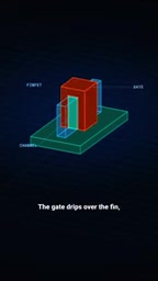
FinFET's success proved the value of three-dimensional structures, but engineers didn't stop there—if three sides aren't enough, then four.
Gate-All-Around: The Ultimate Four-Sided Wrap
The next-generation technology is called Gate-All-Around (GAA). It cuts the channel into extremely thin ribbons (nanosheets), and the gate completely wraps around these ribbon channels, controlling from top, bottom, and both sides simultaneously. This requires new material systems and manufacturing processes, such as selective etching in alternating silicon-germanium and silicon layers to release suspended silicon ribbons.
GAA further improves gate control, allowing shorter channel lengths and lower leakage current. From planar to FinFET to GAA, the logic of transistor evolution remains consistent: bring the gate closer to the channel and wrap it more comprehensively.
Engineering Challenges and the Future
GAA manufacturing is significantly more difficult, involving complex steps such as atomic layer deposition, selective etching, and 3D integration. Additionally, stacking multiple channel layers can increase drive current, but thermal management and parasitic capacitance issues still need optimization.
The changing shape of transistors is essentially a game between control and leakage. When planar structures reach their limit, three-dimensional wrapping becomes inevitable. In the future, 2D materials or vertically stacked devices may continue this trend, but the core principle remains: better control, less leakage.
One-line Summary
From planar to FinFET to gate-all-around, the core of transistor evolution is wrapping the gate more fully around the channel to suppress leakage.
Paragraph Summary
Starting from "a transistor is a voltage-controlled switch," the article explains how the gate controls current on/off by forming a channel beneath the insulating layer. As transistors shrink, the source-drain distance becomes too close, causing the short-channel effect; planar transistors still leak severely when off, making power and heat unacceptable. To solve this, FinFET makes the channel a vertical fin, letting the gate control from three sides; the next-generation gate-all-around (GAA) cuts the channel into ultra-thin nanosheets so the gate wraps all around, further enhancing control but also introducing manufacturing challenges like atomic layer deposition, selective etching, and 3D integration. The article notes that the changing shape of transistors is essentially a game between control and leakage; future 2D materials or vertically stacked devices may continue this trend, with the core principle always being better control and less leakage.
Related articles

M&M's Spent Millions Replacing Artificial Blue Dye — Why Is It So Hard?
Mars spent millions trying to replace artificial blue dye in M&M's with spirulina, but thick material clogs pipes and residue risks mold, forcing a full production-line rebuild. Here's the engineering behind the reformulation.

Teammate Wanted for Meta Global AI Developer Hackathon: Computer Vision & Medical AI
A Reddit developer seeks teammates for the Meta Global AI Developer Hackathon, focusing on computer vision and medical AI. This article analyzes the track logic, skills-complementarity needs, and topic selection strategy behind this teaming signal.
Multiple Claude Models Hit by Errors: A Postmortem of Fable 5.1, Sonnet 5.5, and Haiku 5.5
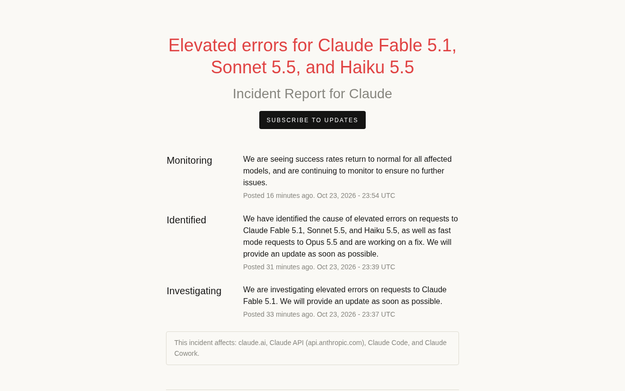
Claude Fable 5.1, Sonnet 5.5, Haiku 5.5, and Opus 5.5 fast mode saw elevated errors; Anthropic identified and resolved the issue in 17 minutes. This postmortem covers the timeline, the technical reasons for the multi-model cascading failure, and practical lessons for retry and degradation strategies.